Lab 6 - EE 420L
3/27/2019
Pre-lab work:
- This
lab will utilize the ZVN3306A and ZVP3306A MOSFETs.
- Review
these datasheets and become familiar with these transistors.
- Verify
that the simulations seen in lab6_sims.zip reasonably model the behavior
of the transistors' ID v. VGS, ID v. VDS, and gm v. VGS curvers.
- Finally,
watch the video single_stage_amps and review
single_stage_amps.pdf
- Below
are schematics for NMOS and PMOS source followers
amplifiers (also known as common-drain amplifiers)
- In
your lab report discuss the operation of these circuits.
- Simulate
the operatioin of these amplifiers.
- Hand
calculate, and then verify your hand calculations with experimentation and
simulations, the gains and the input and output resistances ensuring that
your test signals are at a high enough frequency that the caps have
negligible impedance but not so high that the gain is dropping off.
- If you build this circuit using electrolytic
capacitors, assuming the input AC signal swings around ground, put
the "+" terminal of the cap on the gate of the MOSFET. Please
indicate, in your lab report, that you understand why the capacitor is
connected this way.
- In
your lab report discuss, in your own words, how to measure the input
resistance.
- For measuring the input resistance add a resistor
equal to the value you calculated between the input voltage source and
the amplifier.
- Measure the peak AC current through this added
resistor by taking the difference in the peak AC voltages across the
resistor (on one side is the input voltage signal and the other side is
the connection to the amplifier's input capacitor) and then dividing by
the resistor's value.
- Measure the peak AC voltage on the input of the
amplifier (the left side of the capacitor).
- Dividing this peak AC voltage by the peak AC current
through the added resistor is the amplifier's input resistance.
- Again,
in your lab report discuss how to measure the output resistance.
- For measuring the output resistance, add a resistor
equal to the value you calculated in series with a big capacitor (to
avoid messing up the biasing) from the amplifiers output to ground.
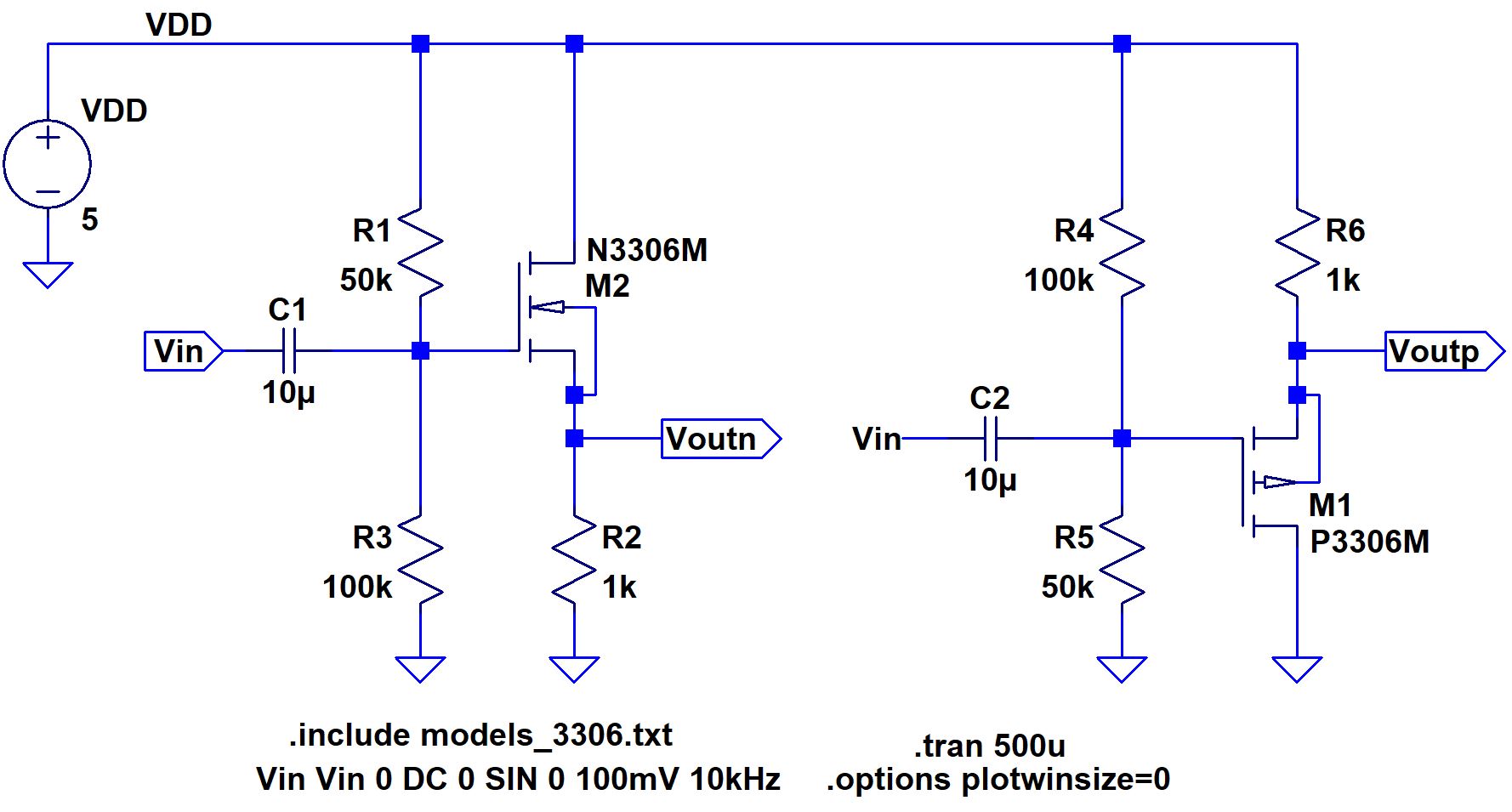
Common Drain Amplifier
This is the schematic for the first circuit
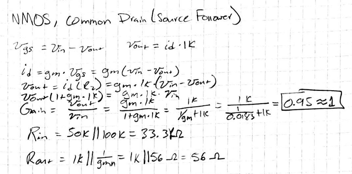
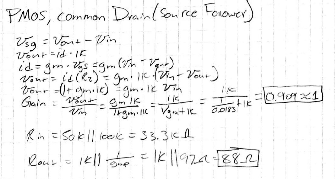
 these are
the hand calculations me and my partner did for DC and AC
these are
the hand calculations me and my partner did for DC and AC


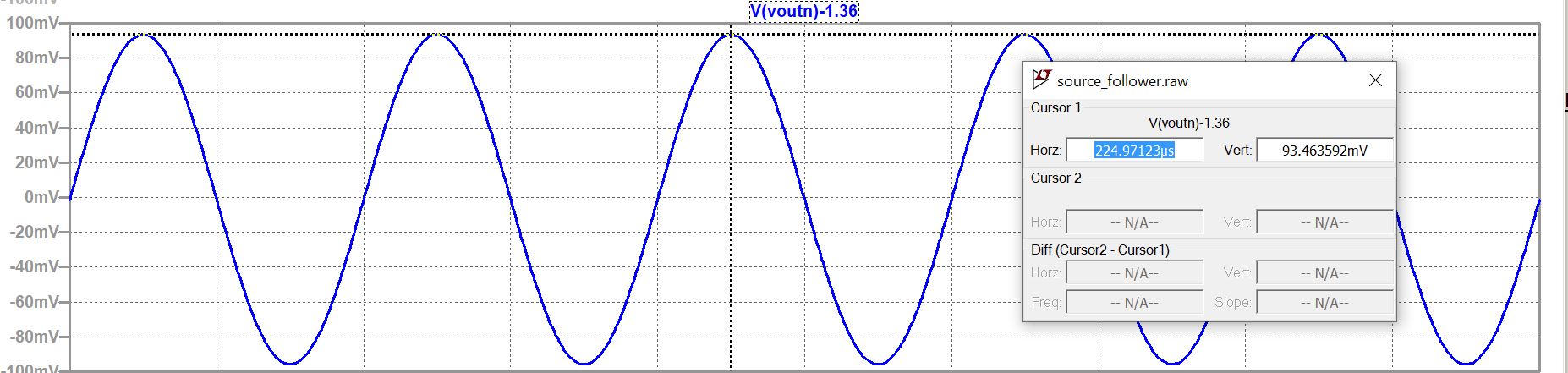
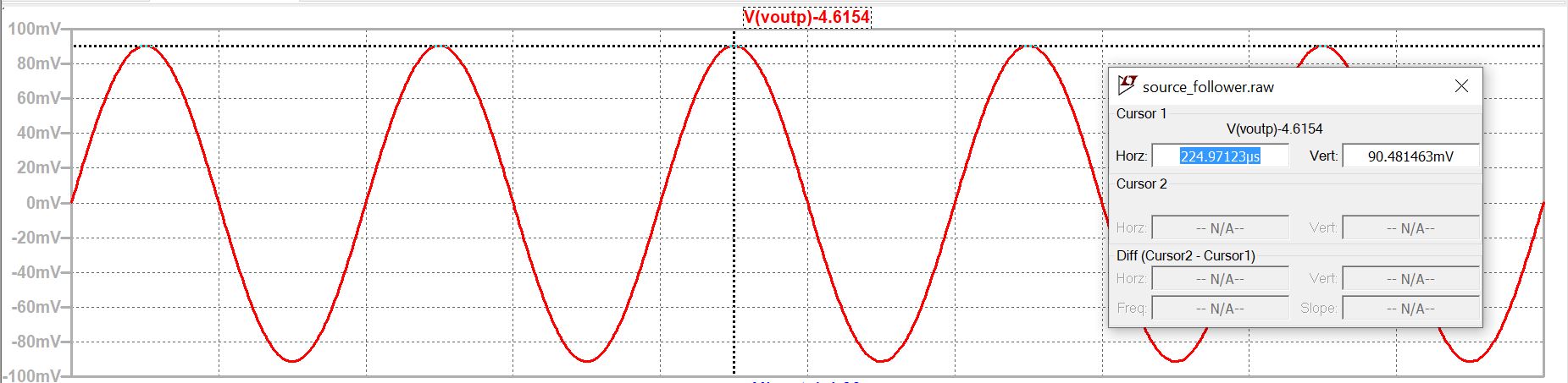
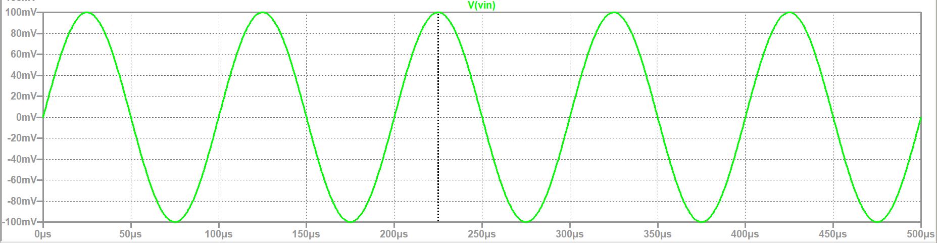
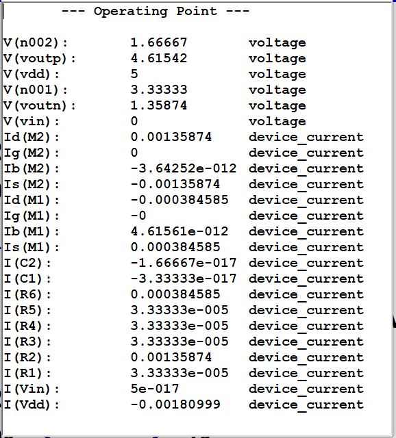
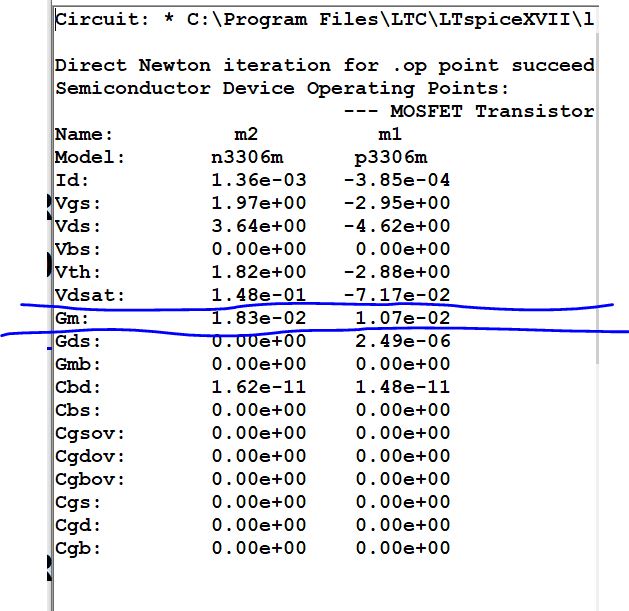
DC simulation
We built the circuit with electrolytic capacitors and put the "+"
terminal at the gate of the MOSFET. We did this because the other orientation
would cause the interior plates to breakdown. The AC voltage will cause an
unwanted reaction unless the positive terminal is connected to the higher
potential DC voltage.
If we use the calculated
values for Rin and Rout and connect them to the output resistor in parallel, we
should get half of the gain we get with nothing connected.
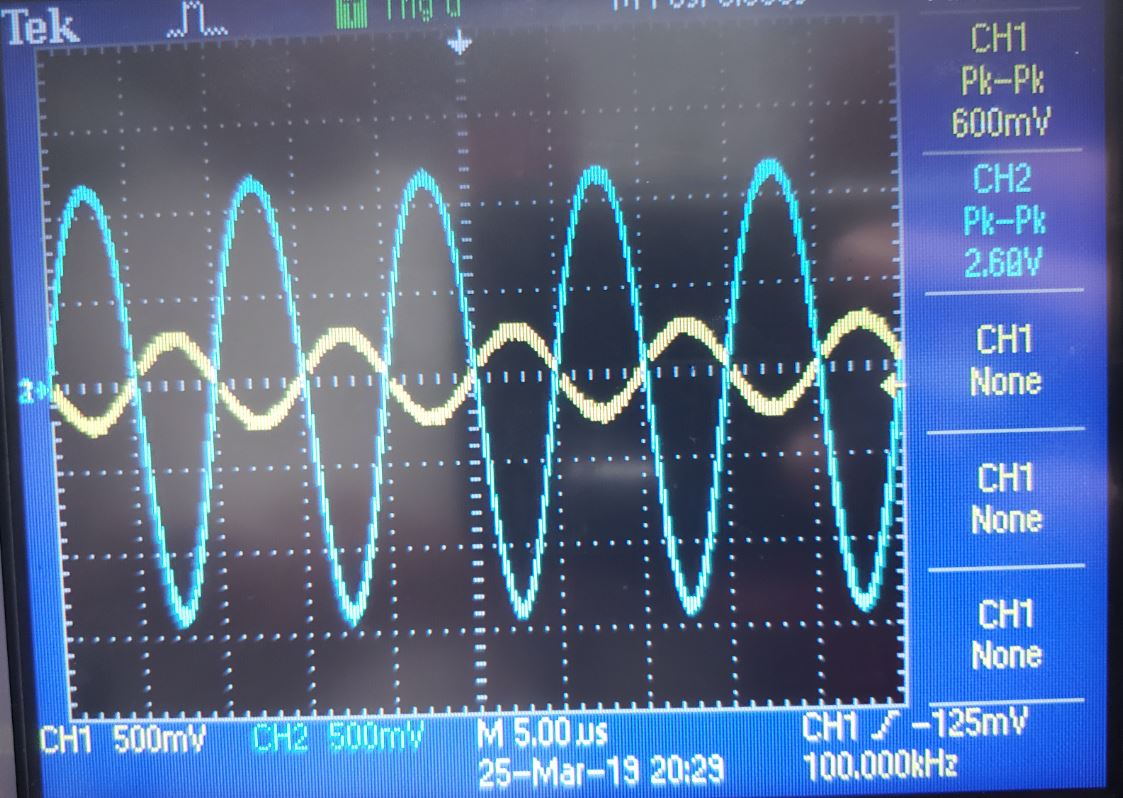
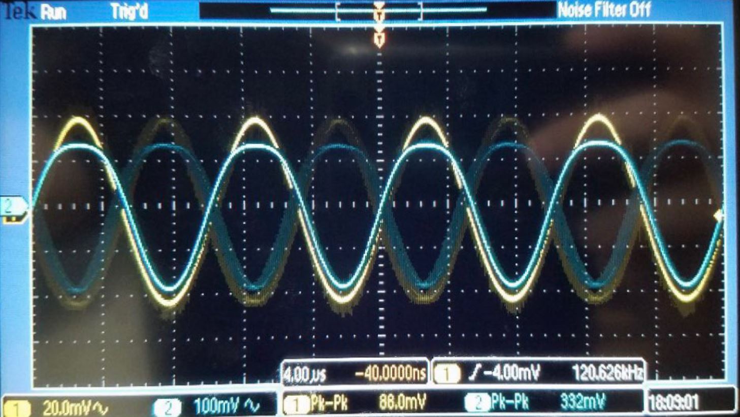
This is a table of the gains and Rin Rout measurements of the MOSFETS
|
NMOS |
PMOS |
|
|
GAIN |
|
|
|
RIN |
|
|
|
ROUT |
|
|
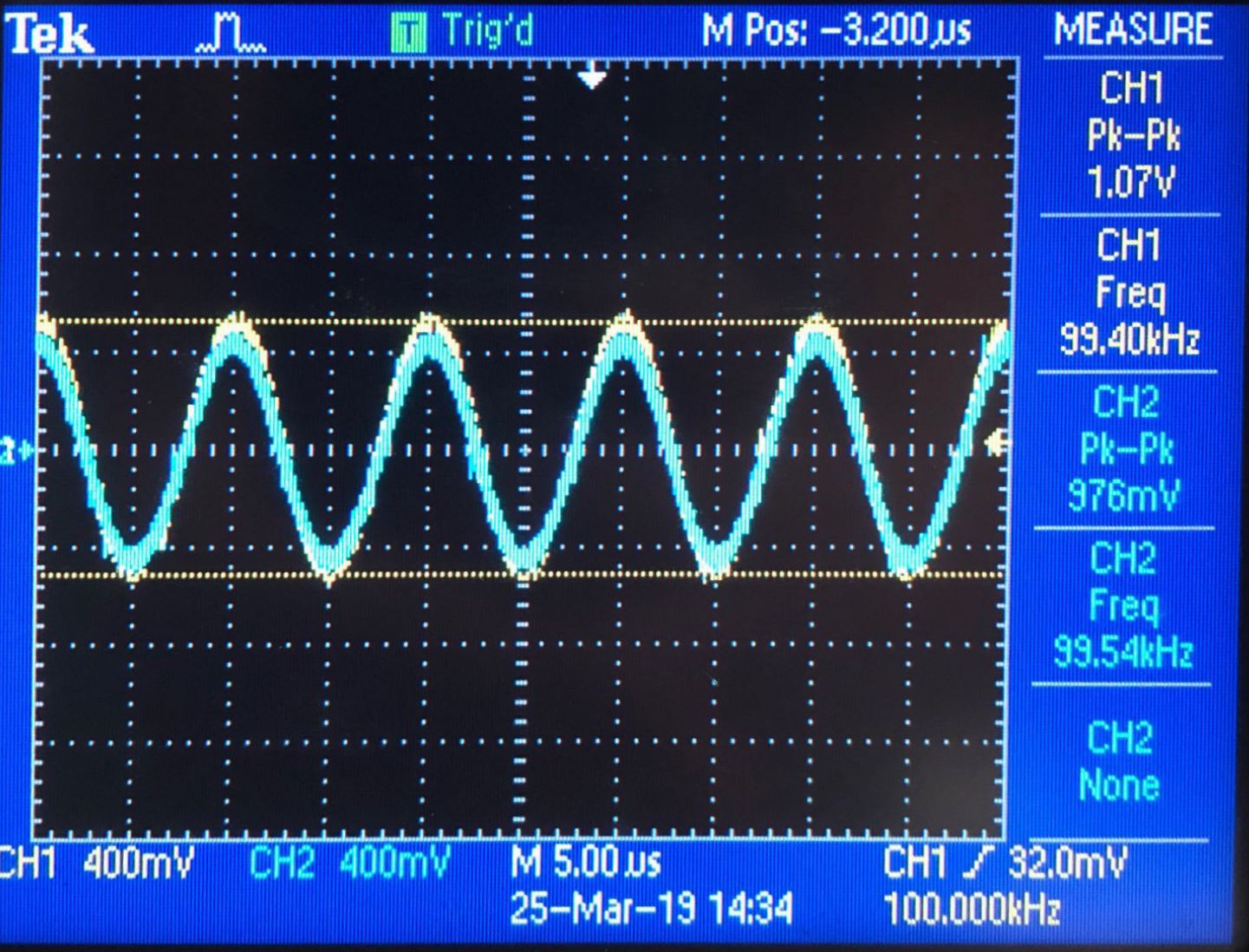
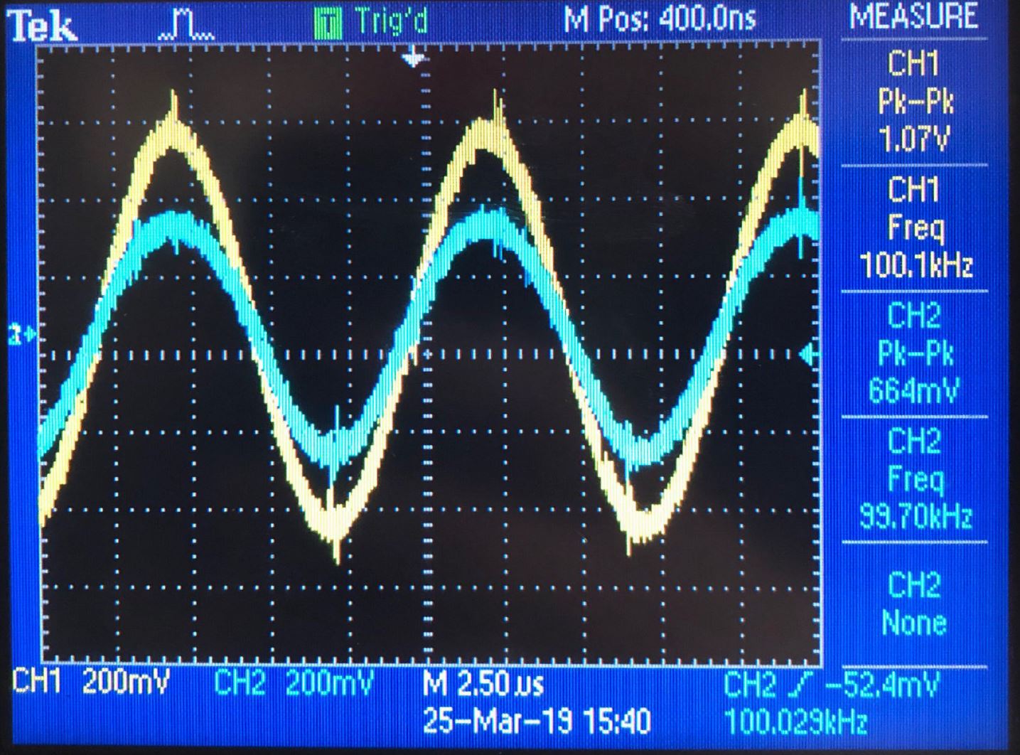
This is a table of all the gains of the NMOS and PMOS. We had trouble with the
experimental values being accurate and even switched out the MOSFETS a couple
times. The results looked worse, but we ended up sticking with this because it
looked the best.
|
HAND |
EXP |
Rin |
Rout |
|
|
GAIN NMOS |
1V/V |
0.91 V/V |
33.3Kohm |
56ohm |
|
GAIN PMOS |
1V/V |
0.62 V/V |
33.3Kohm |
88ohm |
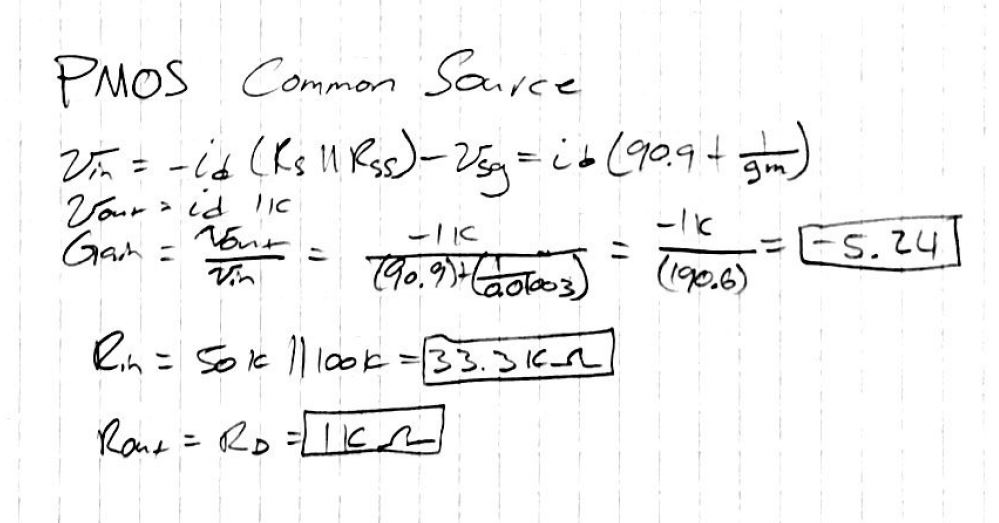
Common Source Amplifier
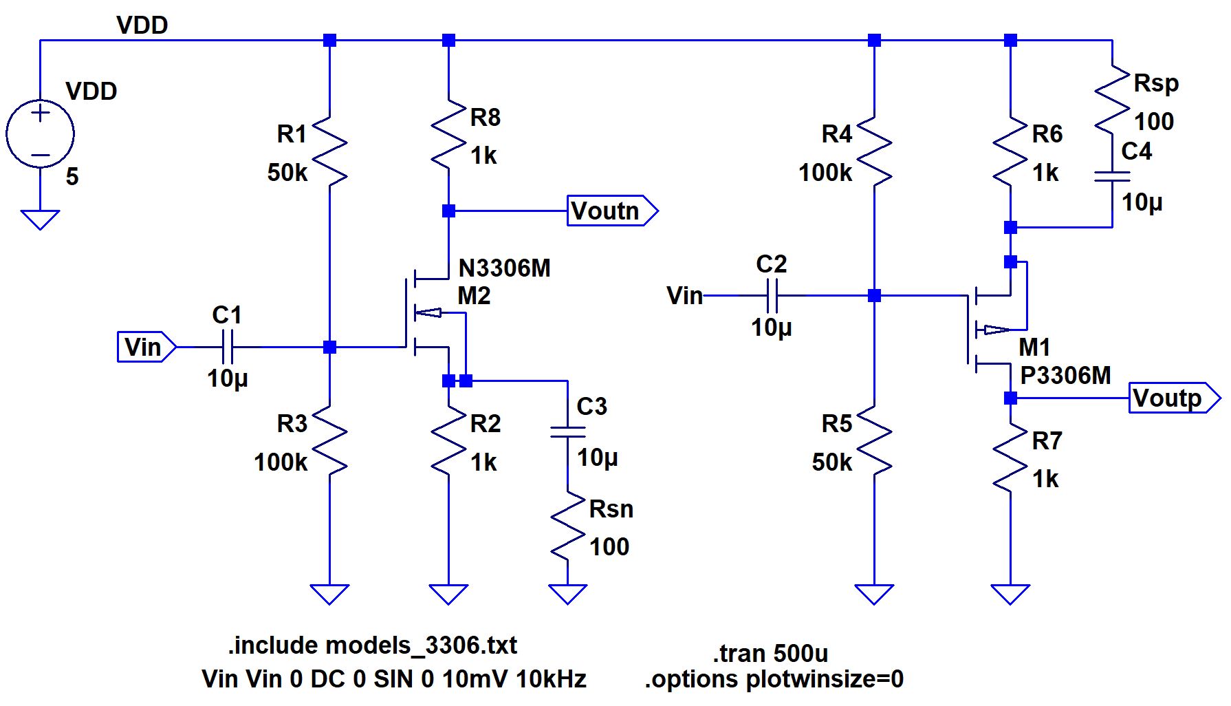
this is the schematic
for the common source amplifier
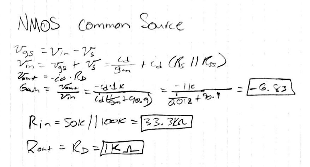
 these are the hand calculations
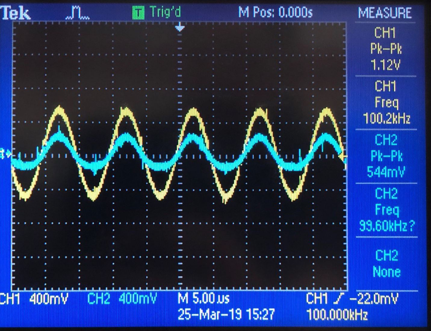
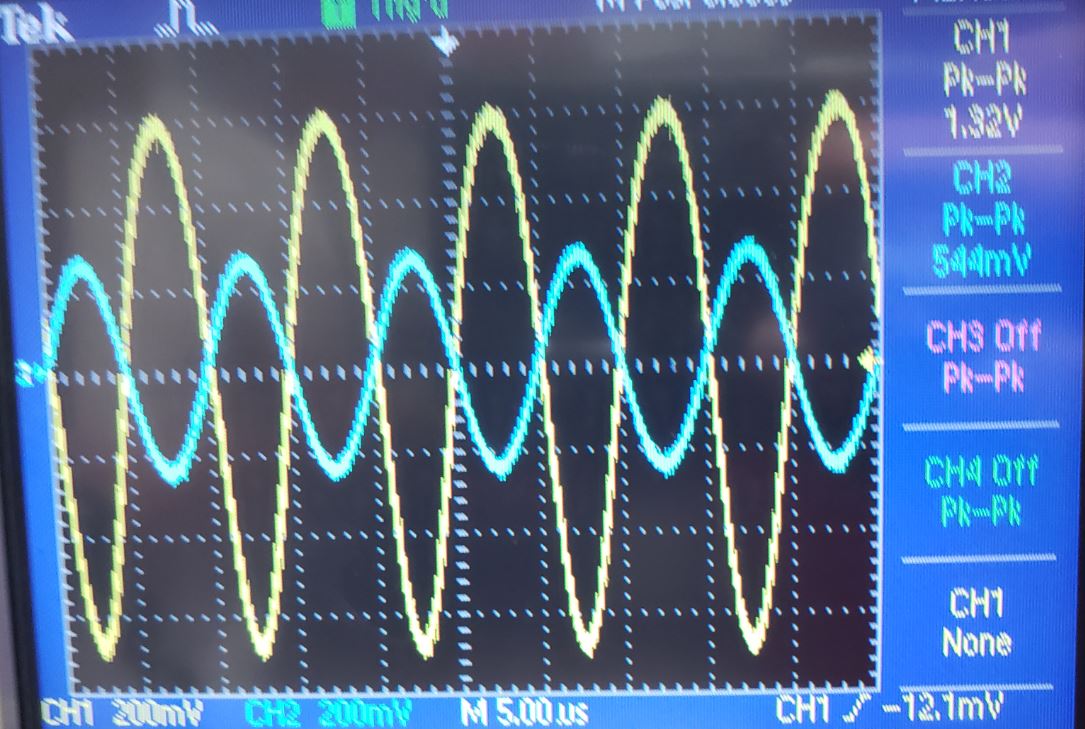
These are the simulated wave forms
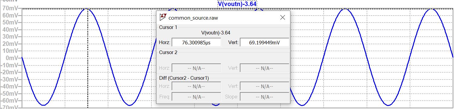
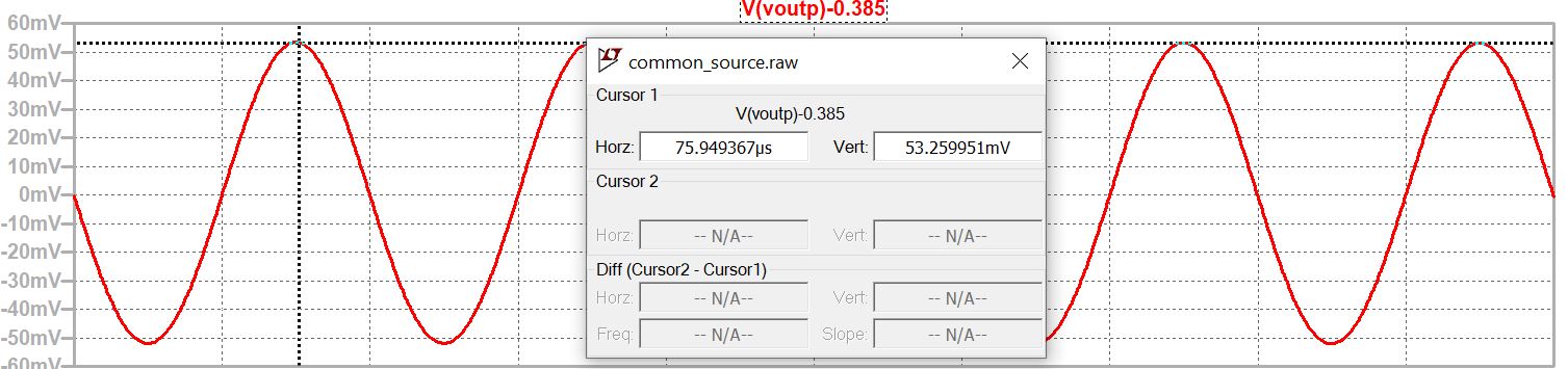
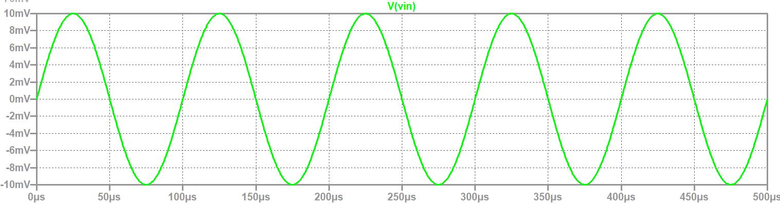
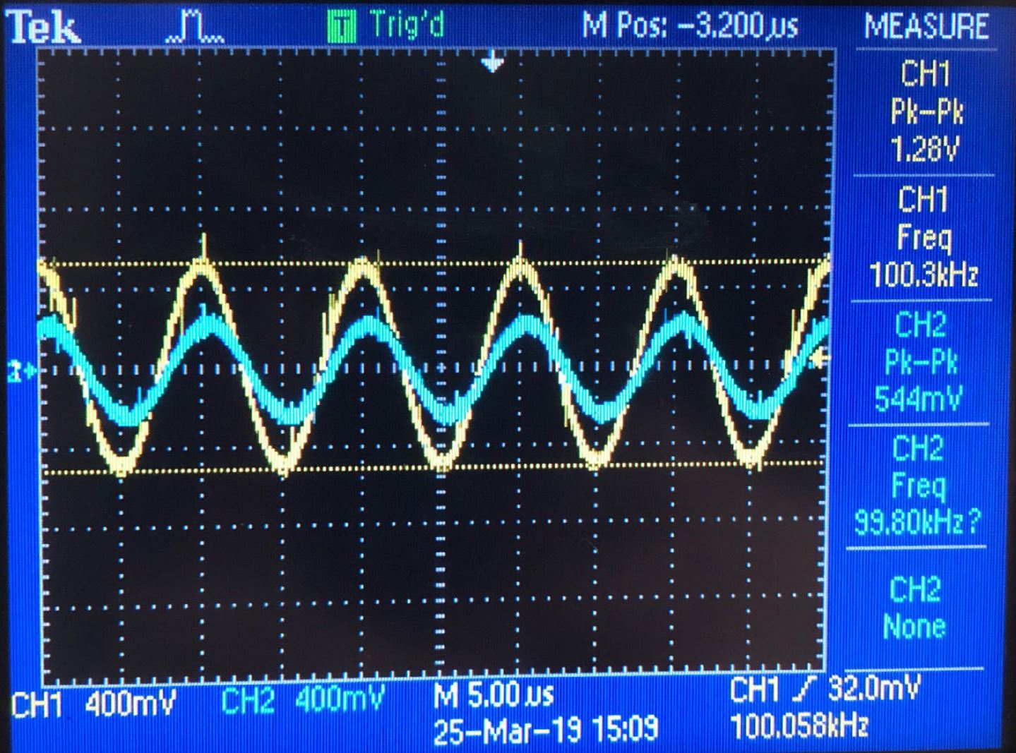
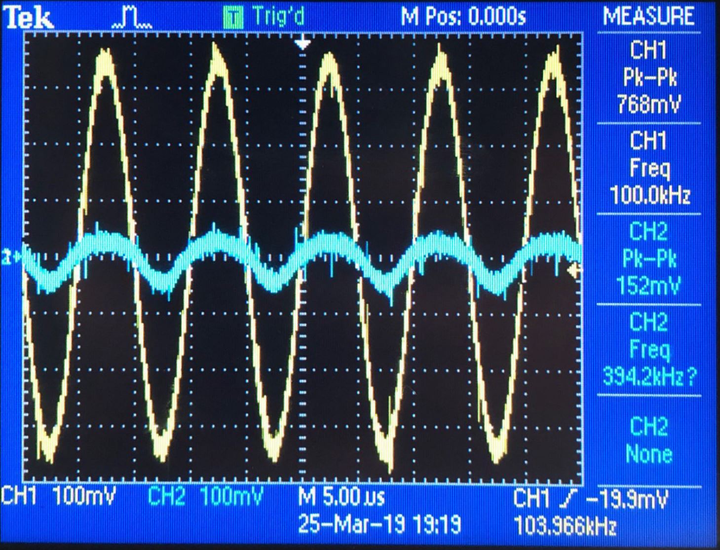
This is the experimental
measurements set up the same as the first experiment.
|
NMOS |
PMOS |
|
|
GAIN |
|
|
|
RIN |
|
|
|
ROUT |
|
|
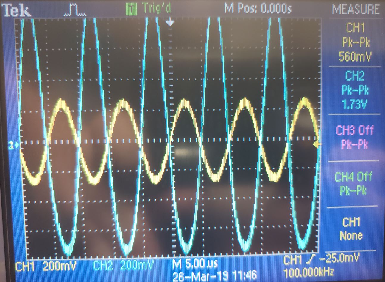
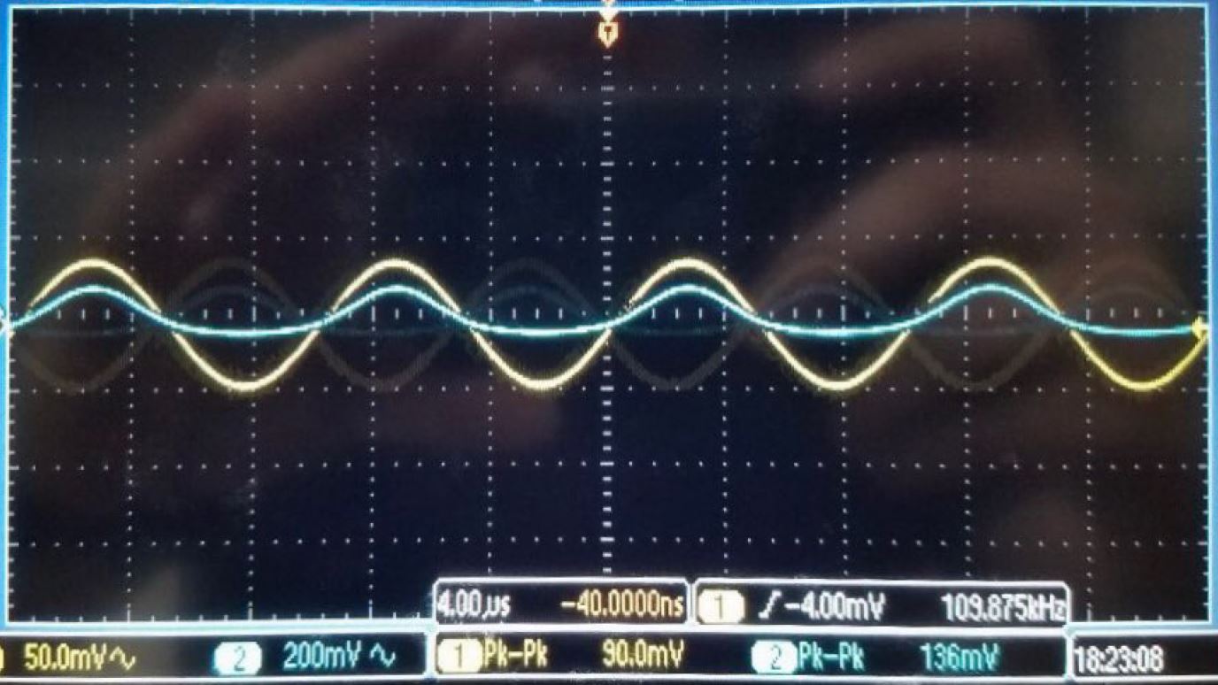
This is the table of our
resuts
|
HAND |
EXP |
Rin |
Rout |
|
|
GAIN NMOS |
6.83V/V |
4.3V/V |
33.3Kohm |
33.3Kohm |
|
GAIN PMOS |
5.24V/V |
3.08V/V |
1Kohm |
1Kohm |
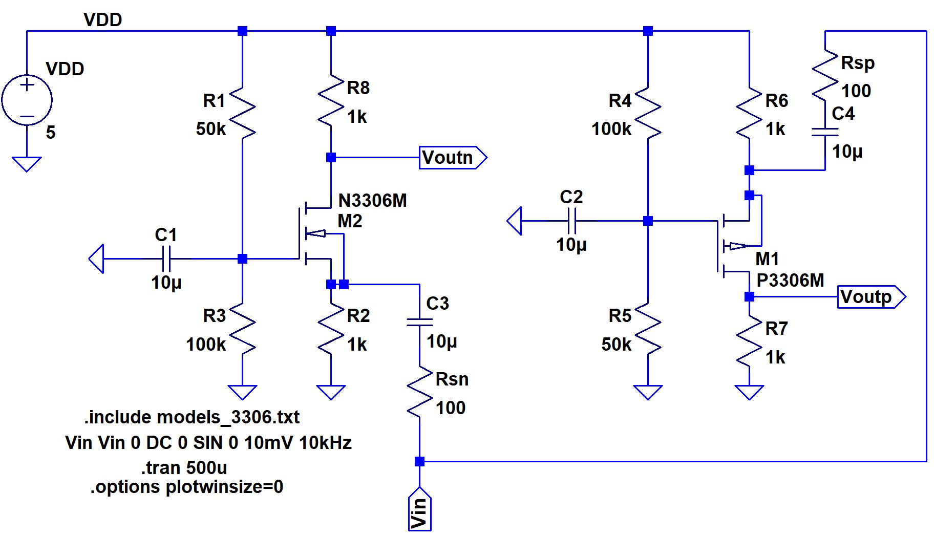
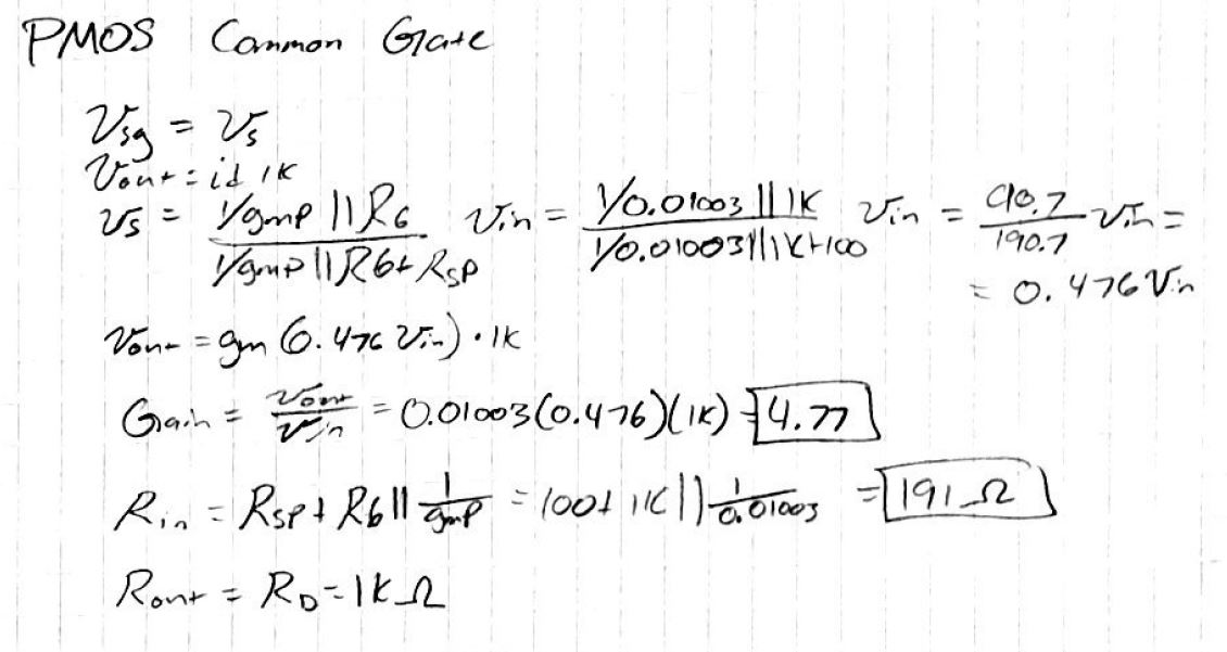
Common Gate Amplifier
this is the schematic for the common gate amplifier
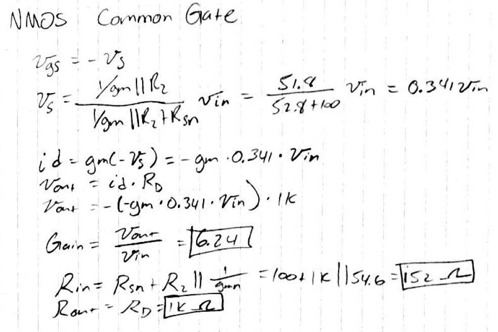
 these are the hand calculations
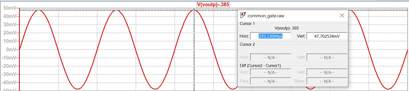
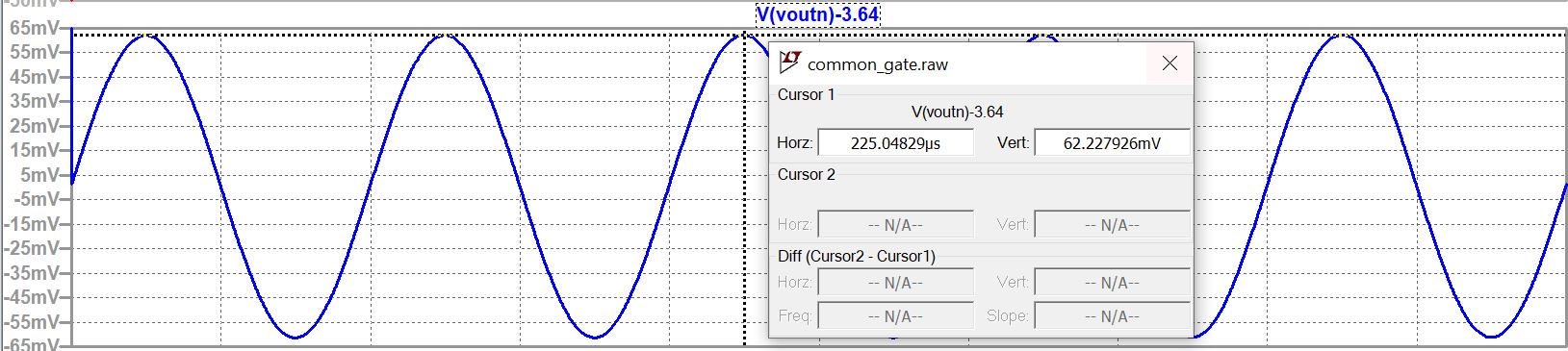
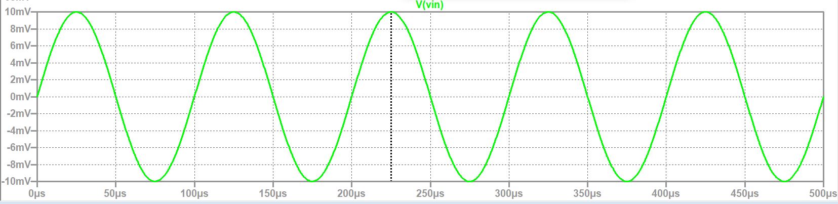
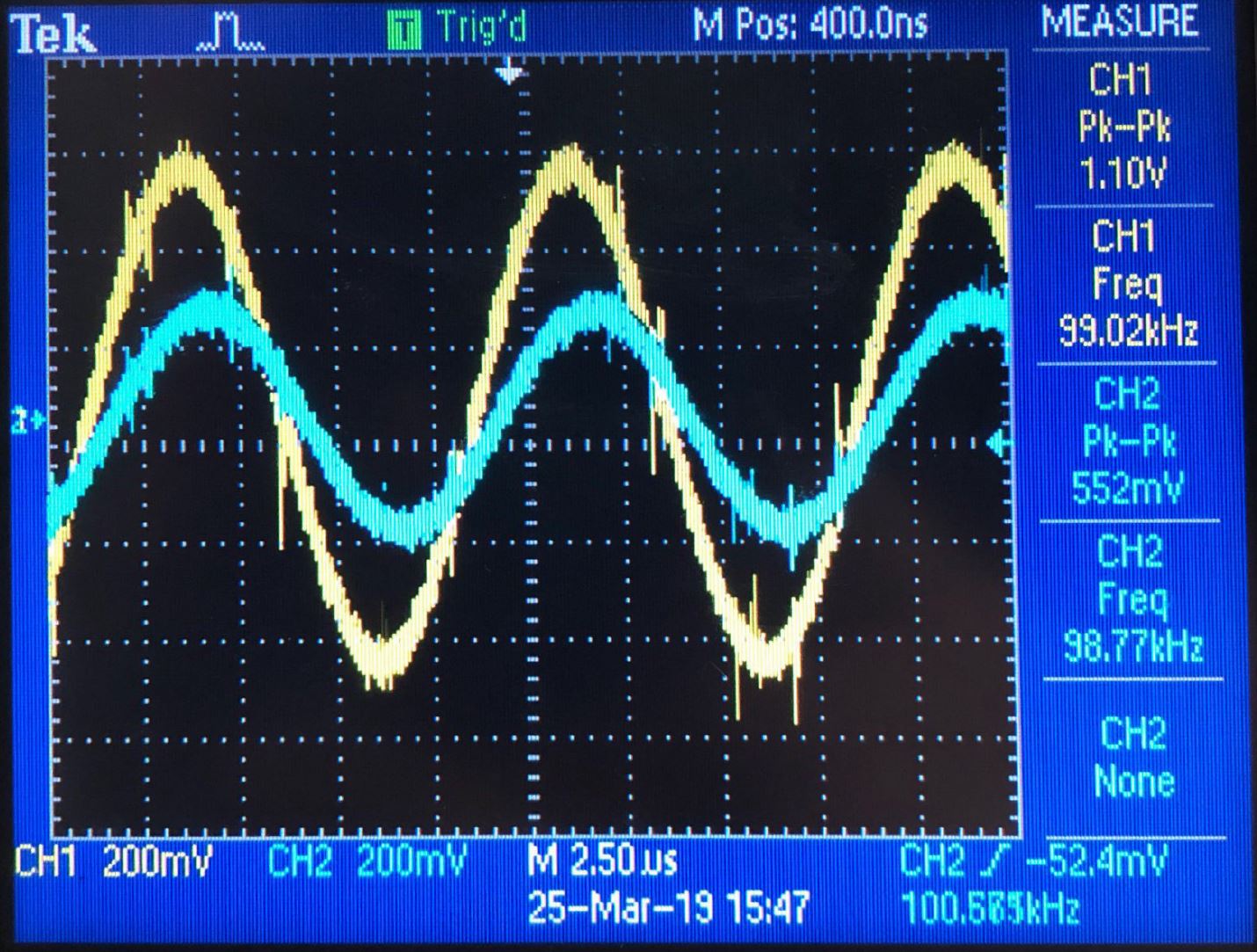
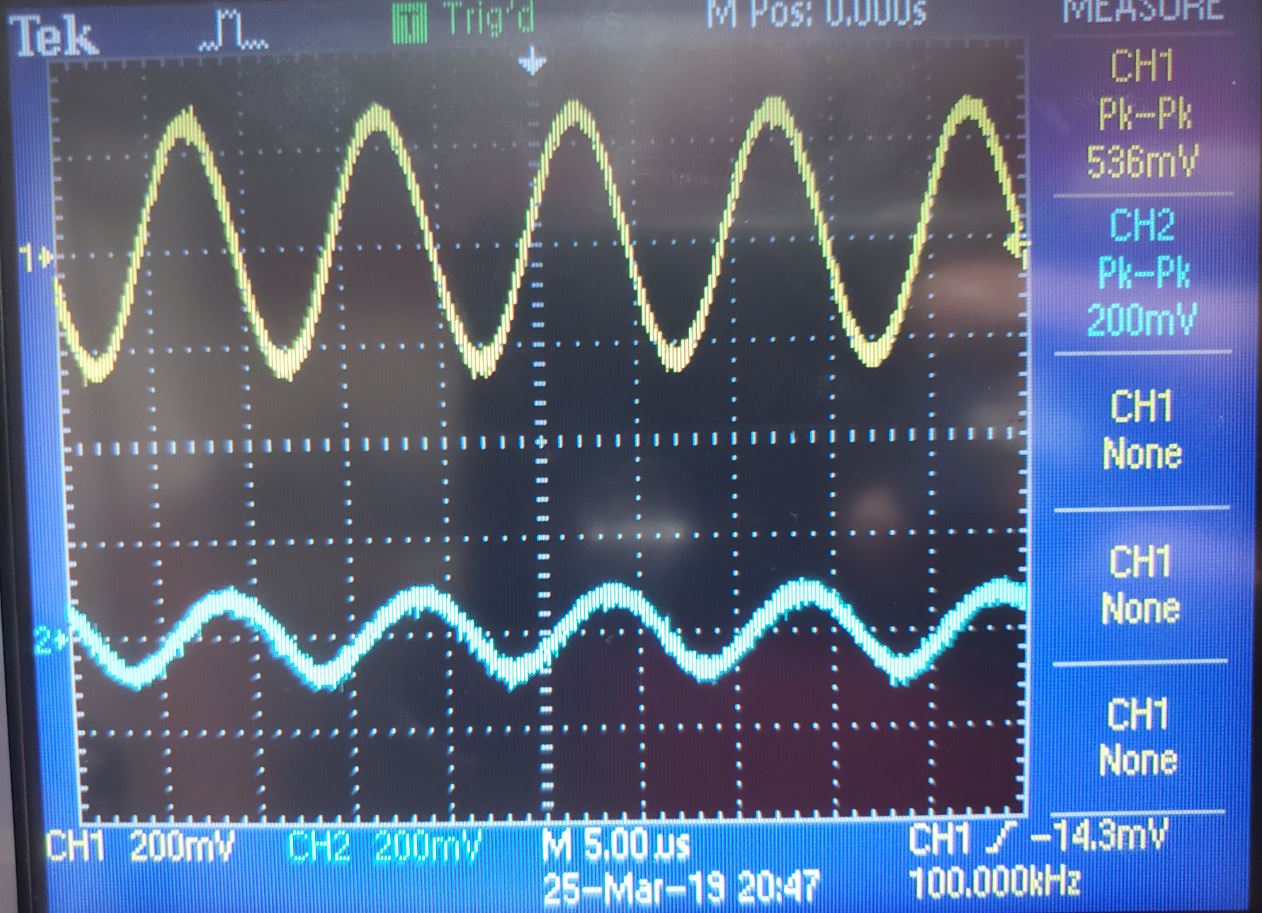
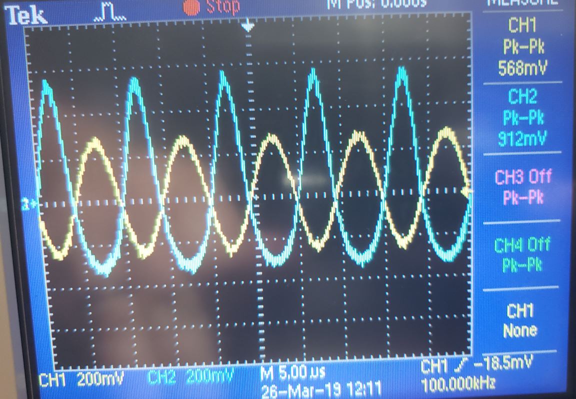
This is the experimental measurements set up the same as the first experiment.
|
NMOS |
PMOS |
|
|
GAIN |
|
|
|
RIN |
|
|
|
ROUT |
|
|
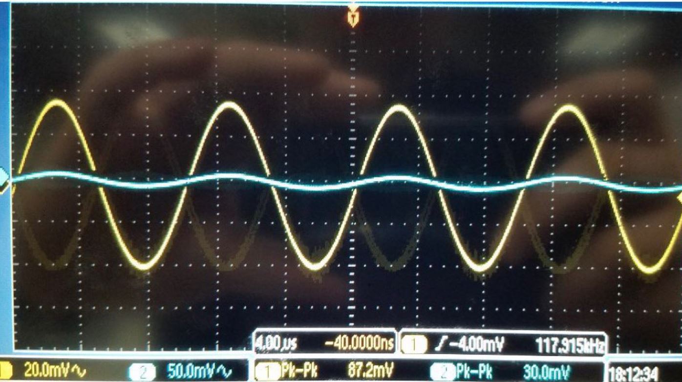
This is the table of our
results
|
HAND |
EXP |
Rin |
Rout |
|
|
GAIN NMOS |
6.24V/V |
3.77V/V |
152ohm |
191ohm |
|
GAIN PMOS |
4.77V/V |
1.5V/V |
1Kohm |
1Kohm |
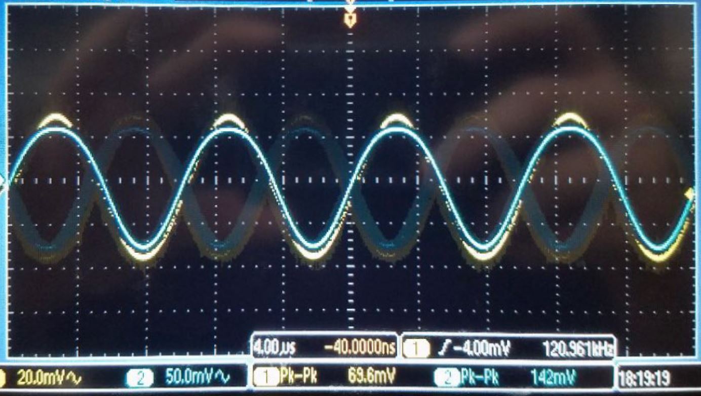
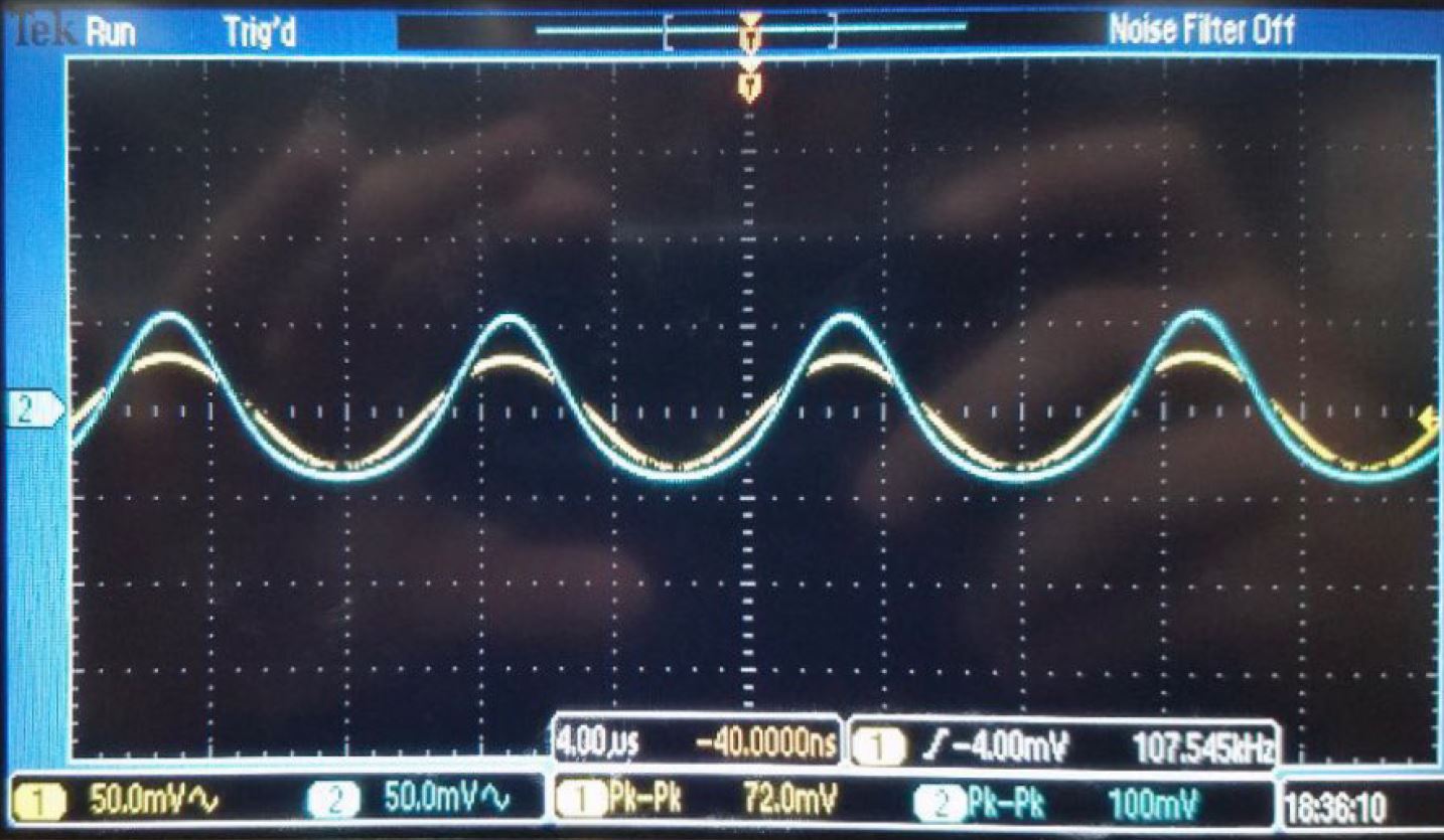
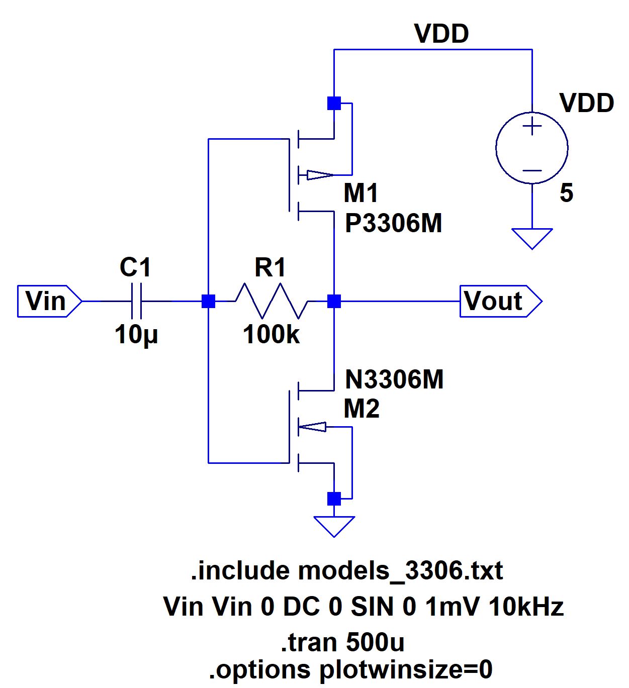
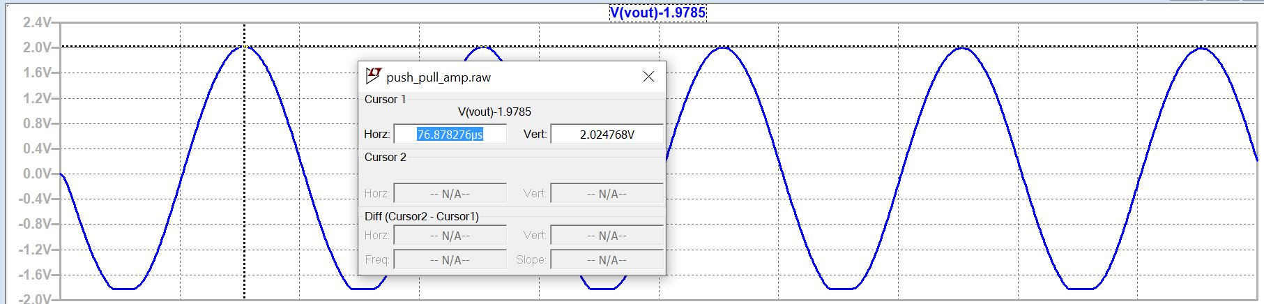
Push Pull Amplifier
this is the schematic for the push pull amplifier
Simulations:
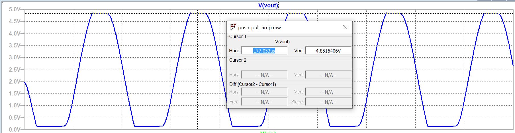
100k:
510k:
Do you expect this amplifier to be good at sourcing/sinking current? Why or why
not?
I expect the amplifier to do well at this because PMOS are good at sourcing and
NMOS are good at sinking.
What happens to the gain if the 100k resistor is replaced with a 510k resistor?
Why?
The gain is much larger with the 510k resistor. The gain is so much larger its hitting the rails and that is whey it is flat on top and
bottom.
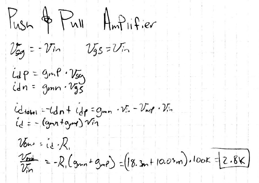
Hand Calculations:
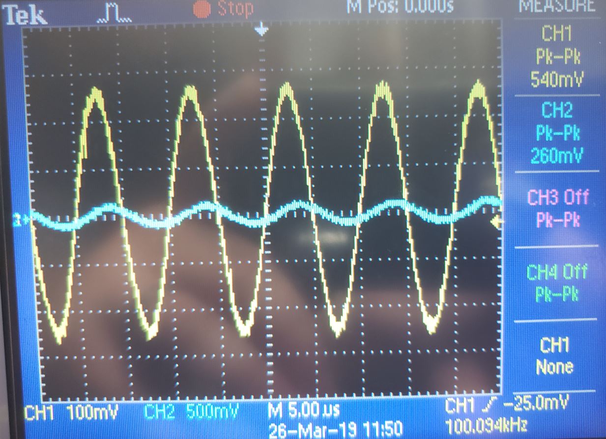
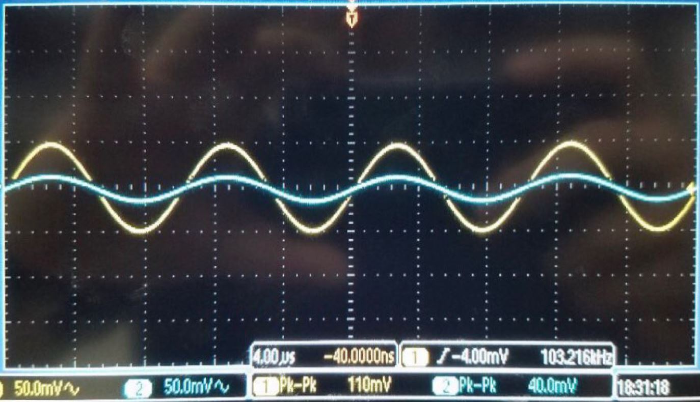
This is our experimental measurement.
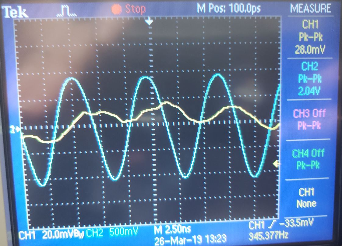
The hand calculations showed that the gain to this amplifier should be around
2.8K, but we could barley get a gain of 72. We tried
multiple MOSFETS which all gave us different values, but this was the only one
that gave a decent gain.
|
HAND |
EXP |
|
|
GAIN |
2.8KV/V |
2.04/0.028 = 72V/V |
Conclusion:
This lab is for us to
gain a better understanding of amplifiers and what the different types might be
used for.