EE 420 Final Project
5/8/19
Assignment: design a voltage amplifier using the ZVN3306A or ZVP3306A
MOSFETs and as many resistors and capacitors as needed.
The requirements are:
1.
Gain of 10
2.
As fast a design as possible driving a 1k load
3.
An input resistance greater than 50k
4.
As large of output swing as possible.
5.
Can pass a 100 Hz input signal.
6.
Can draw no more than 1 mA from a +9 V supply voltage
7.
Detail design considerations
8.
Give measured results showing the amplifiers performance
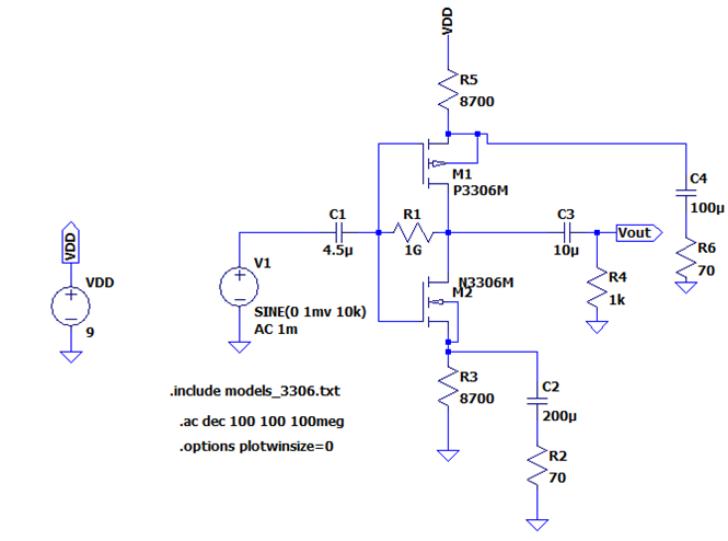
First, I decided to use a push pull amplifier
topology, with added resistors to the sources of the MOSFETs to reduce power
dissipation. I used two resistors in parallel in order to have a DC biasing
resistor as well as one for the AC signal.
I picked resistor values in order to find a
calculated gain of 10 to begin my design.
Below are the calculations showing a gain of 10.
Calculations
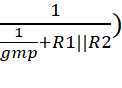
Find idn:
![]()


Find idp:
![]()


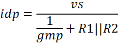
Add both
currents together:
![]()
 +
+ 
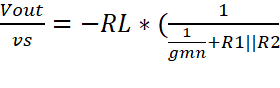
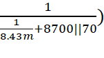
Vout = -Rl * iout
 +
+
 +
+
 +
+ 
 +
+ 
![]() +
+ ![]()


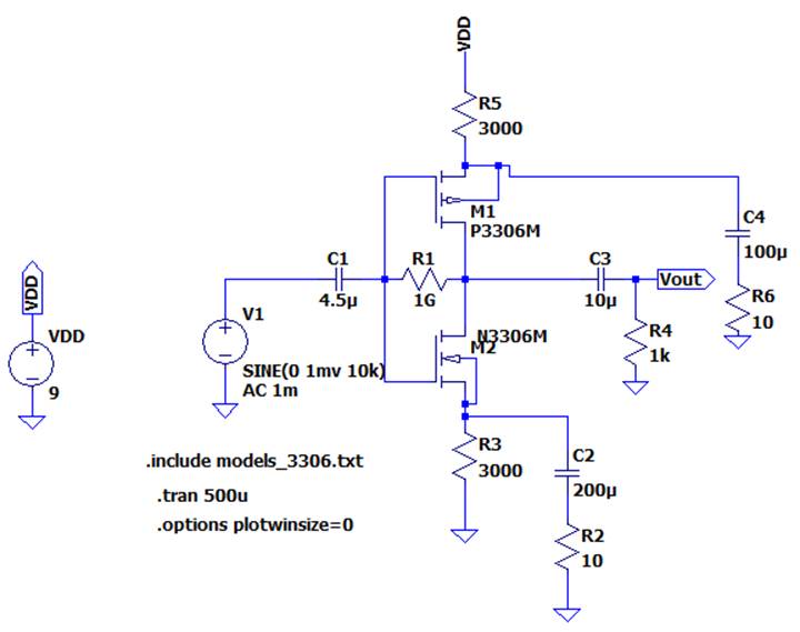
Because the
values generated a gain of 10 in the calculations, an LTSpice simulation was
used to confirm the calculations. The simulation also produced a gain of 10.
|
My design, giving a gain of 10. |
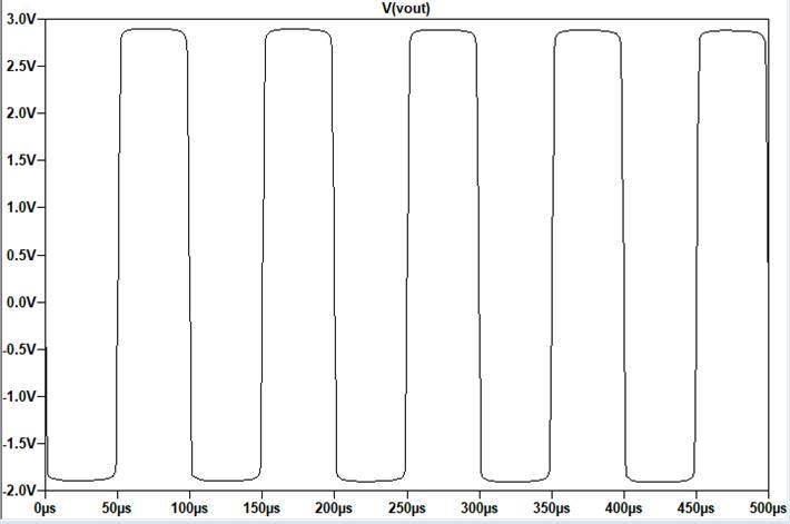
Input signal is 1mV and output
is 10mV, showing a gain of 10. |
|
|
|

The input
resistance was found by measuring the current over the input signal and
dividing the amplitude of the signal by the current.
The input
resistance was well over 50kohms, at 80Mohms.
The output
swing of the circuit was found by inputting a large amplitude into the sine
wave input and measuring the swing. The output swing in the simulations is
4.4V.
|
Input resistance more than 50k |
Output Swing of 4.4V |
|
|
|
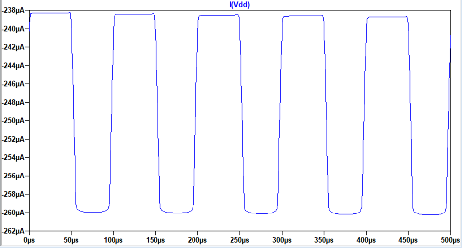
To find the
quiescent current over the 9V voltage source, the wire connecting VDD to the circuit
was disconnected and the current was measured. The current was 238uA, which is
well under 1mA, satisfying the conditions.
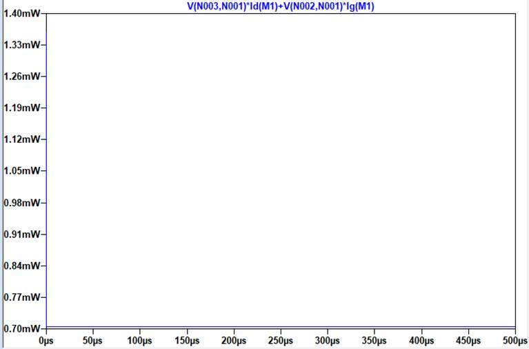
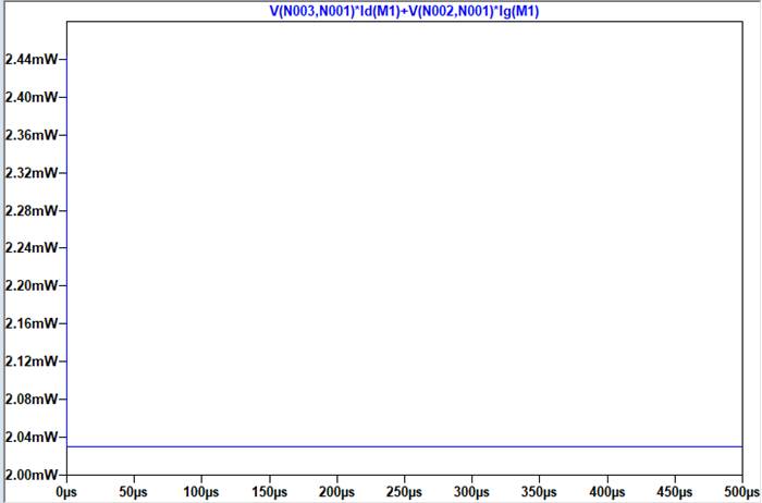
The power
dissipation was also measured to be 1.40mW when the circuit starts up, moving
down to 0.70mW. The maximum power these transistors can withhold is 625mW, and
the power this circuit is dissipating is much less than the maximum value.
|
Current no more than 1mA. |
Power dissipation less than
625mW. |
|
|
|
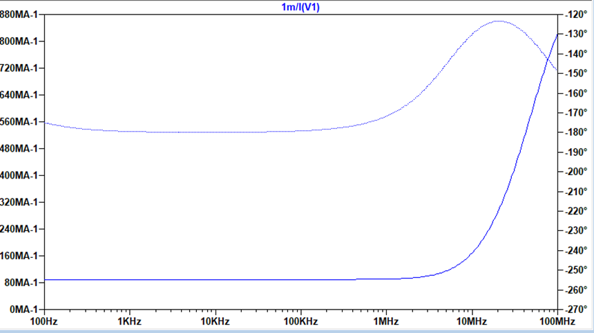
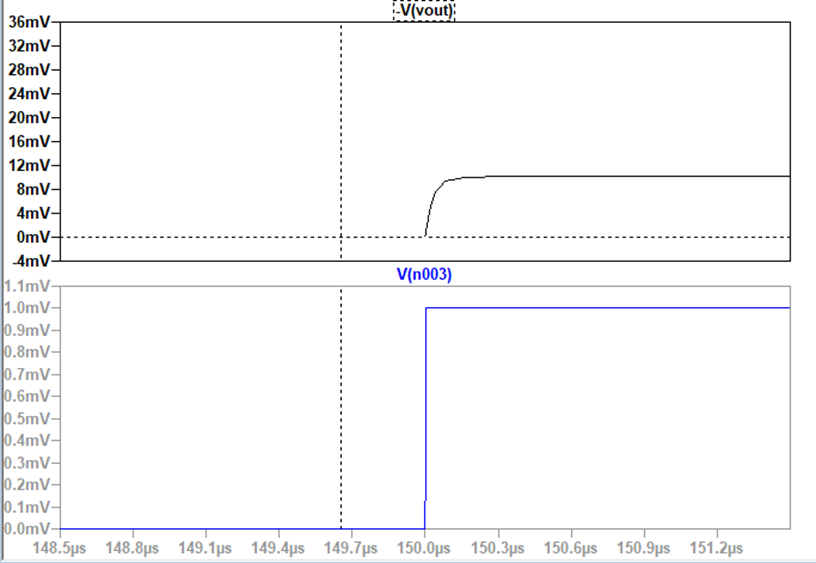
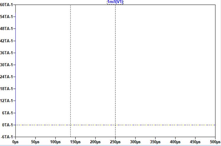
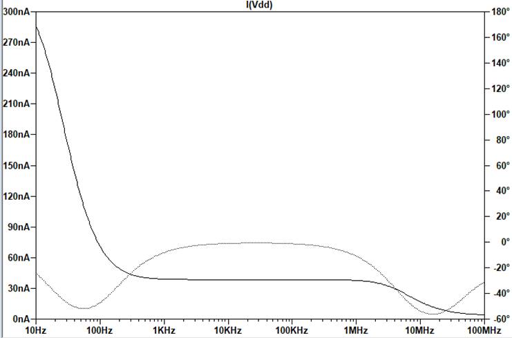
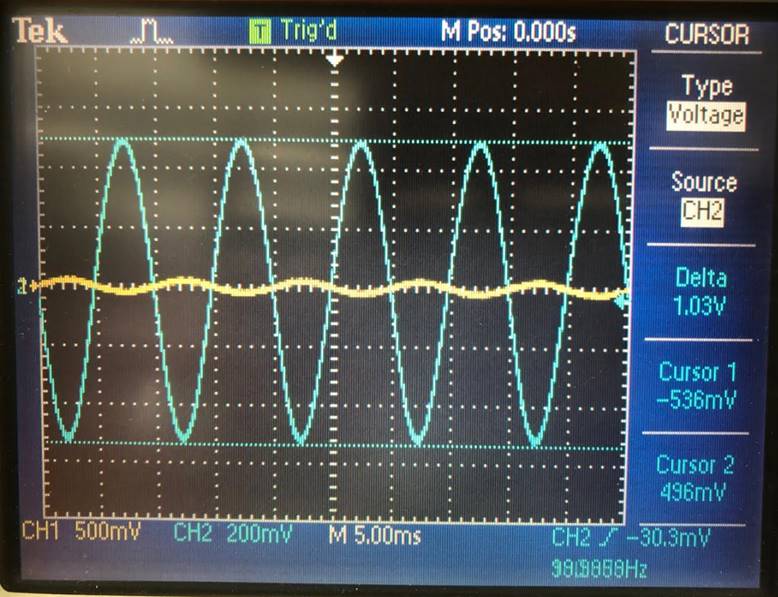
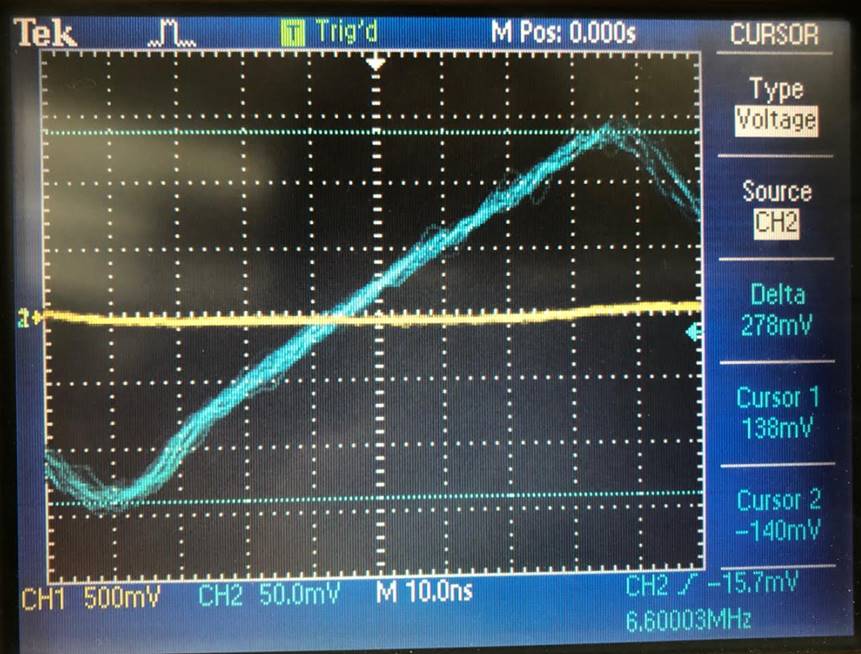
A signal that’s as fast as possible, shown using
slew rate. It reaches a speed of about 5MHz before it rolls off in the
photo on the right.
Slew rate = 2*
pi * frequency * peak voltage
The signal
responds very quickly to the input, shown in the window at V(n003). This means
that the slew rate is very fast and that the amplifier performs at a quicker
rate.
Since the
signal stays at 10mV until about 5MHz, it performs well at very high
frequencies.
|
Showing the slew rate, it rises
and flattens out quickly, showing that it is fast enough. |
It reaches a speed of about
5MHz before it rolls off. |
|
|
|
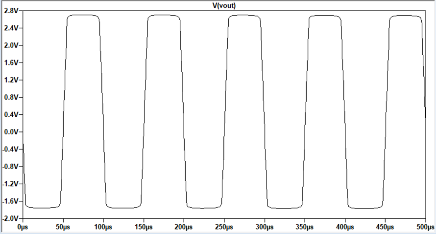
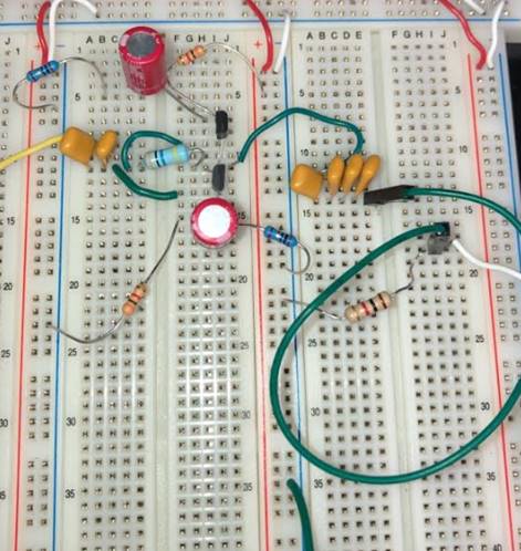
EXPERIMENTAL RESULTS WITH CIRCUIT ABOVE
Since the circuit performed well and matched all specifications given
in the project, and the calculations matched the LTSpice simulation, the
circuit was built on a breadboard and measured experimentally. Unfortunately,
the gain was reduced by a factor of 2, down to a gain of 5 instead of a gain of
10. The results of the circuit above are as follows:
|
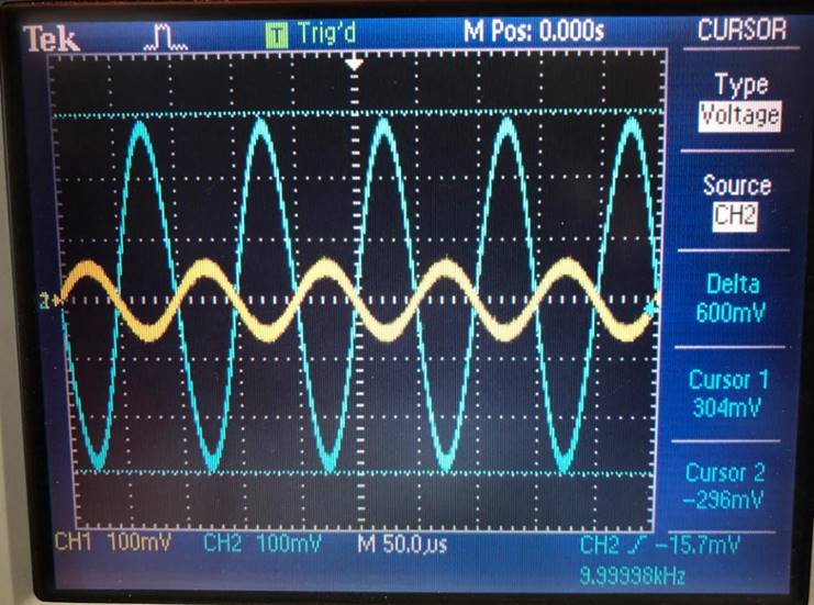
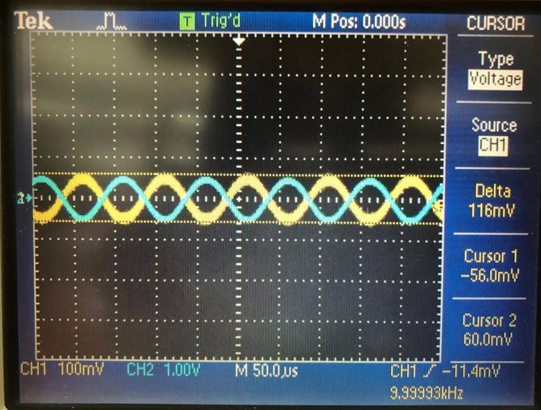
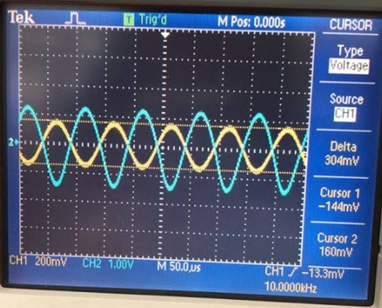
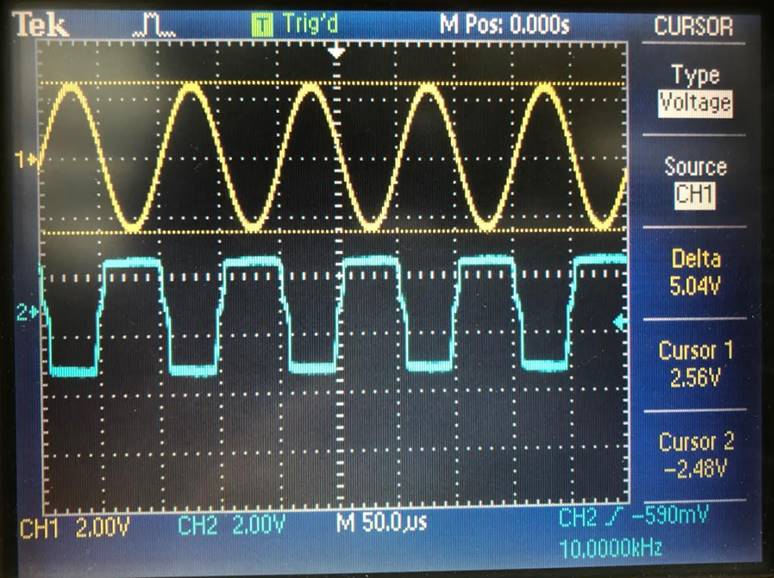
Input of 100mV (132mV) |
Output of 600mV, Gain of 4.545 |
|
|
|
|
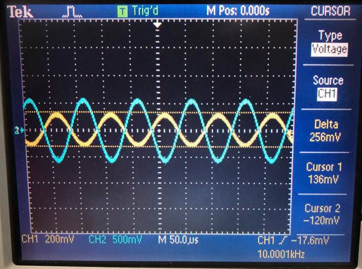
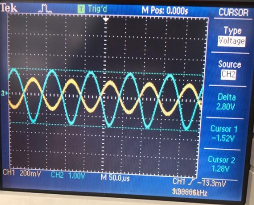
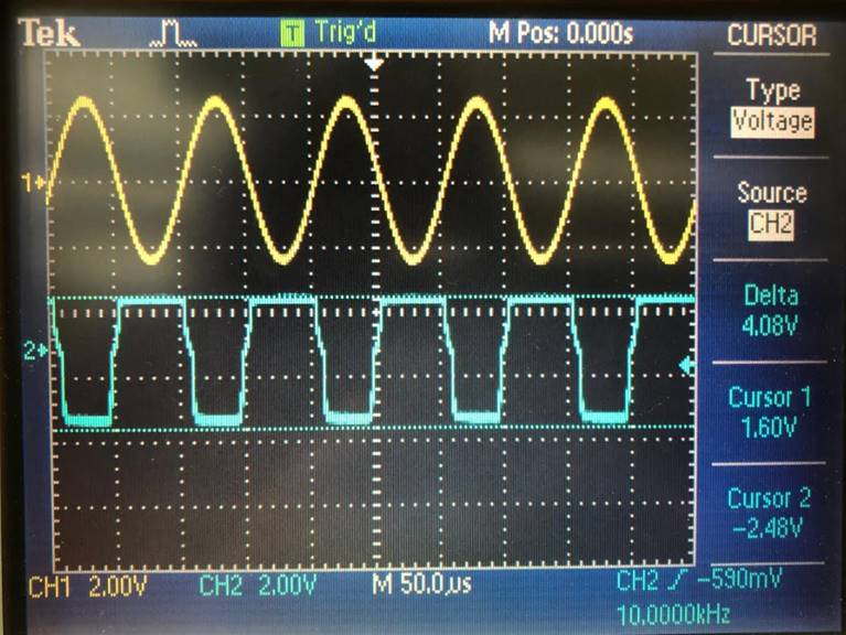
Input of 200mV (256mV) |
Output of 1.20V, Gain of 4.6875 |
|
|
|
|
Input |
Output |
Gain |
|
132mV |
600mV |
4.545 |
|
256mV |
1.20V |
4.6875 |
In the
experiment above the gain I was receiving was only half of the calculated and
simulated gain of 10. Since I was losing a gain of 5, I calculated for a gain
of 15 to compensate for the 5 that I lost previously. In my LTSpice simulation
using these values, I received a gain of 20. In the real experiment, the gain
was 5 less than what I calculated, giving me a gain of 10 as expected.
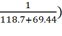
First, I
recalculated to find a gain of 15, with hopes that a gain of 5 would be lost in
the experimental circuit because of the variable performance of the transistors
and equipment.
GAIN OF 15:
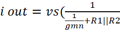
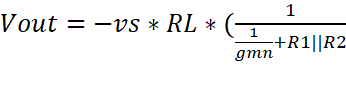
Find idn:
![]()
Find idp:
![]()
Add both
currents together:
![]()
+
Vout = -Rl * iout
+
+
 +
+ 
![]() +
+ ![]()


Since the gain
was about 15, I built the circuit on LTSpice and received a gain of about 20. I
checked each project specification to check the circuits performance now that
the gain in the simulation was double the previous gain. All the specifications
were met with the new circuit as well.
|
Experimental Circuit (for
breadboard) |
Showing a gain of 20. |
|
|
|
With this
design we can see that:
|
The
input resistance is still greater than 50kohms, reaching TeraOhms,
which is a much larger resistance than the previous circuit’s. |
It pulls a gain of 20 over
100Hz. |
It pulls less than 1mA from a
9V power supply. |
|
|
|
|
The output
swing was 1 V larger, however the power dissipation was more than double the
previous circuit. The power dissipation was still far below the maximum so it
was not a problem.
|
Output swing of about 5V |
Power dissipation less than the
maximum, 625mW. |
|
|
|
Since the specifications
were met in the simulations, I built the circuit on a breadboard to verify the
experimental results.
EXPERIMENTAL
RESULTS using design with a calculated gain of 15 and an LTSpice gain of 20:
Below is a photo
of the circuit on a breadboard circuit.
Just as
hypothesized, the experimental circuit performed at a gain of 5 less than the
calculated gain. Since the calculated gain was 15, the experimental gain was
10.
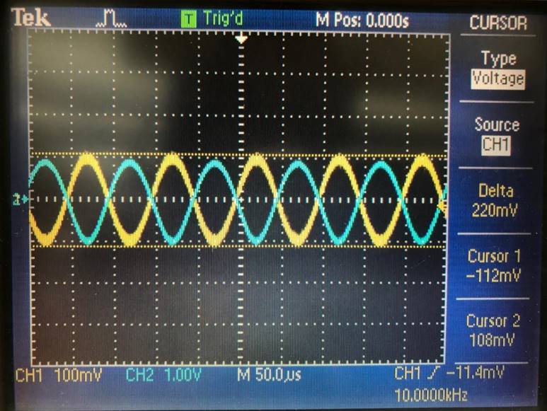
GAIN OF 10
|
Input of 100mV |
Gain of 10 gives |
|
|
|
|
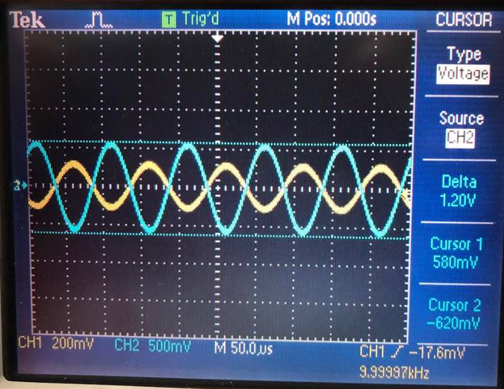
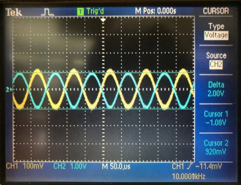
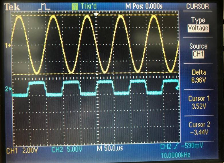
Input of 200mV |
Gain of 10 gives 2.04V. |
|
|
|
|
Input signal of 300mV |
Gain of 10 |
|
|
|
GAIN OF 1O
AT DIFFERENT FREQUENCIES STARTING AT 100Hz
|
Gain of 10 at 100Hz |
Gain of 10 at 100kHz (see channel 2 volts per
division [200mV] for measurement) |
|
|
|
|
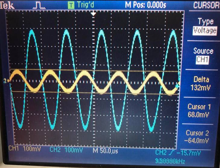
Gain of 10 at 350kHz. |
Gain of 8 at 1MHz (see channel 2 volts per
division [200mV] for measurement) |
|
|
|
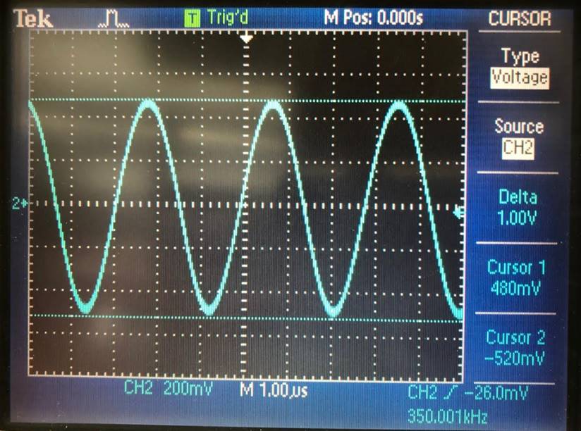
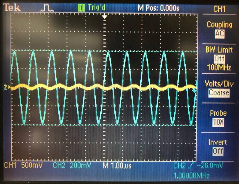
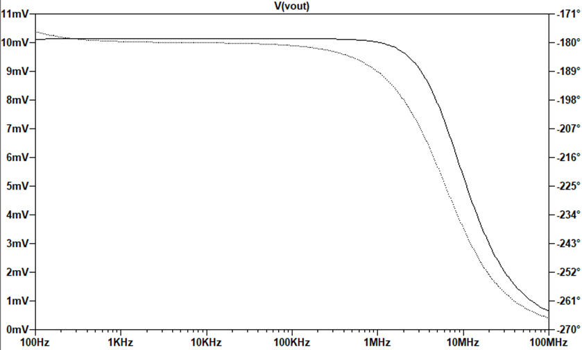
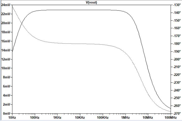
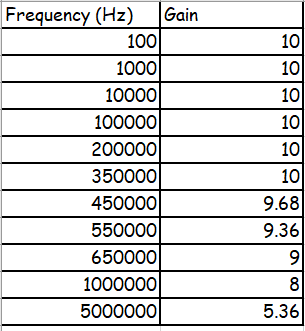
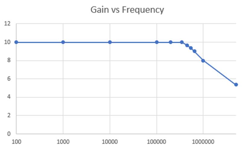
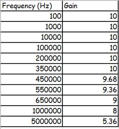
Chart detailing frequency response: the gain remains at 10 until
about 450kHz.
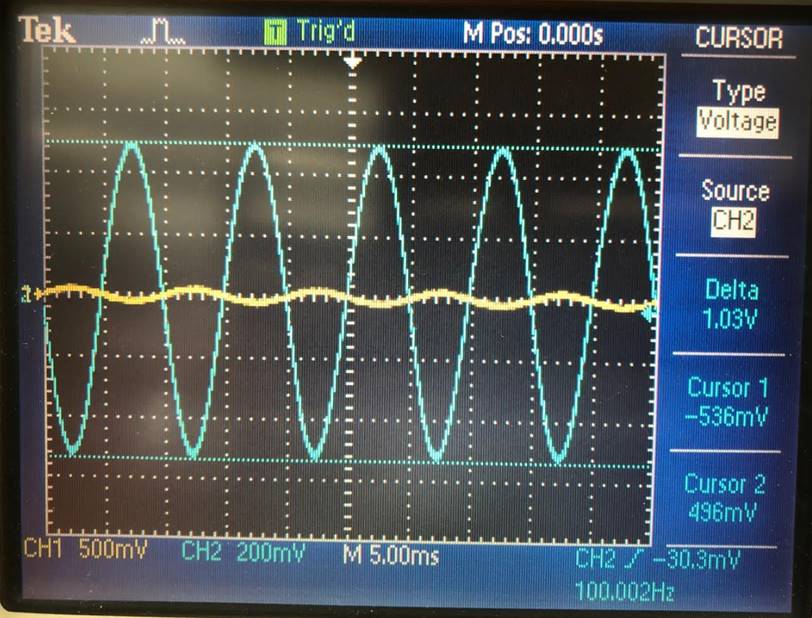
Output swing of 4V:
|
Input signal of 5V |
Output swing of 4V |
|
|
|
|
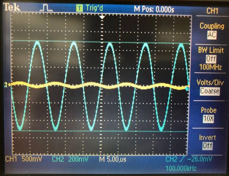
Input signal of 7V |
Output swing of 4V |
|
|
Channel
2 volt per division is 5V and the signal from channel two is a little below
the division, showing that it is at 4V. |
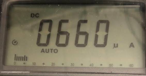
Current from
9V VDD when disconnected from the rest of the circuit: 660uA
The current my design draws with no input signal, under quiescent
conditions, is 660uA which is less than 1mA.
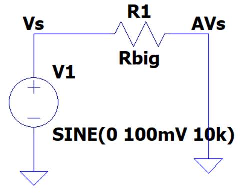
Input
resistance
When given
this circuit where Rbig is 30Meg in the circuit, the
input resistance can be calculated experimentally.
Ideal Rin Calculations:
 which satisfies the requirements of an input
resistance greater than 50kohms.
which satisfies the requirements of an input
resistance greater than 50kohms.
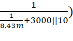
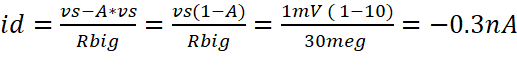
Experimental Rin Calculations:
Vs is the
voltage on the left side of the Rbig resistor, closer
to the input, and vg is the voltage on the right side of the resistor, closer
to the output.
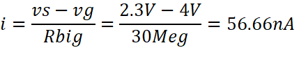
![]() which is greater than 50k ohms
which is greater than 50k ohms
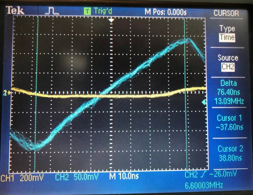
Slew Rate
To find slew rate, you must find the change in voltage over the
change in time.

|
Change
in Voltage |
Change
in Time |
|
|
|
Conclusions and Final Tables:
1. Gain of 10
The factors contributing to the gain are: experimental
gain, simulated gain, and calculated gain.
|
|
Circuit
for Gain of 10 |
Circuit
for Gain of 15 |
|
Calculated Gain |
-10.36 |
-14.98 |
|
Simulated
Gain |
10.1 |
22 |
|
Experimental Gain |
4.6 |
10 |
2. As fast a design as possible driving a 1k load
Slew rate:
The slew rate was ![]() , which is a fast rate
and shows that the design operates very quickly.
, which is a fast rate
and shows that the design operates very quickly.
3. An input resistance greater than 50k
The factors contributing to overall input
resistance are the calculated input resistance and the experimental input
resistance.
|
|
Circuit
for Gain of 15 |
|
Calculated Rin |
3.33 Meg ohms |
|
Experimental
Rin |
41 Meg ohms |
4.
As large of output swing as possible.
|
|
Circuit
for Gain of 10 |
Circuit
for Gain of 15 |
|
LTSpice Circuit |
4.4V |
5V |
|
Experimental Circuit |
3V |
4V |
5.
Can pass a 100 Hz input signal.
Frequency response:
Chart detailing frequency response: the gain remains at 10 until
about 450kHz.

6.
Can draw no more than 1 mA from a +9 V supply voltage
Both designs were able to draw less than 1mA
from the 9V supply voltage input.
7.
Detail design considerations
The biggest concern when designing this circuit
was producing a gain of 10 while also supplying a large output swing, and
drawing less current. I tested a few circuits before settling on the push pull
amplifier, which is the best topology for creating the largest output swing.
Overall, I had to increase my gain by ten in order to arrive at an experimental
gain of 10. The first circuit I built had a gain of ten in calculations and in
the LTSpice simulations, but only had a gain of about
five in real life. Since a gain of 5 was lost, I recalculated to achieve a gain
of 15. The LTSpice simulation showed that the gain
was 20, however, when I built the circuit, it gave a gain of 10. The disparity
between the calculations, simulations and experimental circuits are the result
of random variables such as equipment changes, changes in real life MOSFET conditions,
and other factors that exist in practical circuits. The important thing to note
when designing practical circuits is to plan for a disparity between the
calculations, ideal simulations, and actual experimental circuit. It is near
impossible to have calculations that can predict the outcome of a practical
circuit.