EE 420 L – Engineering Electronics II Lab –
Lab 9
Design of a Beta-Multiplier Reference (BMR) using the CD4007 CMOS transistor array
Authored by: Shadden Abdalla
April 23, 2019
Pre-lab work
- This
lab will use the level=1 MOSFET model created in lab 8 and, again, the
MOSFETs in the CD4007.pdf CMOS transistor array.
- Design
and simulate the operation of a BMR that biases the NMOS devices so that
they have a gm of 20 uA/V
- Use a simple (big) resistor to VDD for the start-up
circuit (explain how the addition of a resistor ensures start-up).
- When the BMR is operating the current in the big
resistor should be much smaller than the current flowing in each branch
of the BMR
- Write-up,
like a homework assignment, your design calculations and simulation
results.
- Ensure
that you show the following in what you turn in:
- Hand calculations
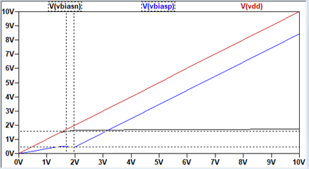
- Operation as VDD is swept from 0 to 10 V
- Vbiasn should stabilize
(be constant) after VDD hits a minimum value (estimate this value of VDD
assuming VGS/VSG is a threshold voltage and VDS,sat/VSD,sat is
zero).
- Vbiasp should follow VDD
after VDD hits a minimum value (show this in simulations)
- Unstable operation if too much capacitance is shunting
the BMR's resistor (see bottom of page 630)
- Comments comparing the hand calculations with the
simulation results
REAL LAB
1. Build your BMR design and characterize it as you
did in the pre-lab (if you use two chips ensure that grounds and VDDs of both
chips are tied together).
Calculations for BMR: Using the values of gm and kpn from our spice models, we can solve for the current and
then use that current value to find the resistor value that we need to build
the BMR. Using the VGS equations we can solve for I, and then rearrange the
equation to find the resistor value.

![]()
![]()
![]()
![]()


![]()
![]()
From the above equation we can deduce that:
![]() which is the
ideal resistor value in this case.
which is the
ideal resistor value in this case.
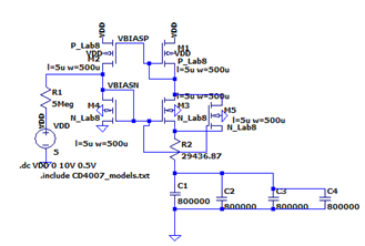
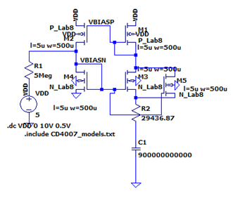
BMR: This is the BMR schematic in LTSpice and on the
breadboard. We used two CD4007 chips for our design. The resistor values that
we used were 32.75kohm and 30.7Mohm. We rounded up for our R1 value instead of
29kohms because we could not find a resistor at that specification.
Below is a snip of the BMR circuit. To the right is the circuit on
the breadboard.


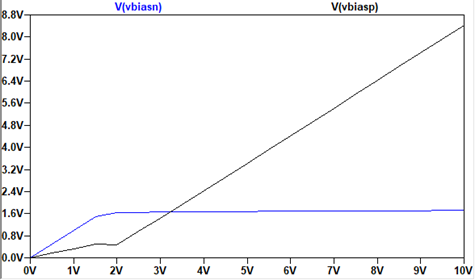
Bias
voltages: Vbiasn and Vbiasp. We measured the bias voltages coming from our
breadboard circuit to ensure that the voltages resulting from the BMR were resonable enough to produce accurate values in the current
mirror and the cascode circuits.
Vbiasn was
1.48V.

Vbiasp was
3.528 V:

Level 1 models used:
We made these models for lab 8. Using these values below, I calculated
the values for the circuit above. The models are very ideal and were changed in
order to provide the best results. They do not fully match the calculations and
were edited in order to give a better result. We used these values to calculate
the current and find the resistor value above. These values were the basis of
the calculations.
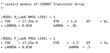
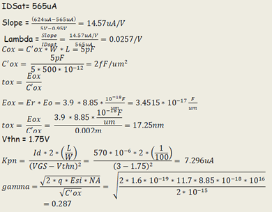
These are the calculations for the NMOS used to make the SPICE
models:
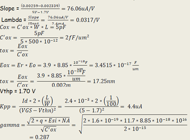
These are the calculations for the PMOS used to make the SPICE
models:
Based on what we estimated, Vbiasn should stabilize after VDD hits a minimum value and
that occurs at about 0.6V. Vbiasp follows VDD after
VDD hits a minimum value, VDSsat.
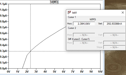
I calculated the current to be about 0.33uA and the simulations
are showing the same using the values from the calculations. That means that
the models are very ideal and the calculations and
simulations are matching well. Typically, that would not happen in real life.
Shunt capacitance affecting circuit:
Adding capacitors in parallel or a
large capacitor does not really change the circuit’s values as seen in the sims
below.

NMOS CURRENT MIRROR
Below is a breadboard photo of both current mirrors:

We used the BMR circuit to produce the bias voltages and inputted Vbiasn to the NMOS current mirror. We created the simplest current
mirror just to display proper operation. We inputted the variable voltage to
the current mirror and measured the drain current on that MOSFET.

Below is the IV curve on the current mirror. It varies from 0 to
2uA over a 0 to 5V range.

EXPERIMENTAL
The IV curve from our measurements below shows similar results to
the LTSpice circuit. This is due to almost perfect SPICE models for our
MOSFETs. The data points we gathered match the LTSpice simulation perfectly.

NMOS CURRENT MIRROR DATA TABLE used to make
graph above:
|
VOLTAGE
(V) |
CURRENT
(A) |
|
0 |
0.102n |
|
1 |
1.70u |
|
2 |
1.73u |
|
3 |
1.79u |
|
4 |
1.84u |
|
5 |
1.87u |
PMOS
CURRENT MIRROR
For the PMOS current mirror, we inputted the vbiasp
voltage into a PMOS with the variable voltage at the source and measured the
drain current on that PMOS. This is almost identical to the setup we used for
the NMOS since the only difference is the gate voltage of the current mirror
and the device.

Below the IV curve shows a range of 0 to 1.4uA of current over the
range of 5V.

EXPERIMENTAL
The IV curve from our experimental values shows a range of about 0
to 1.6uA which is very close to the range found in the LTSpice simulation. This
is due to near perfect SPICE models that mirror the operation of the chip.
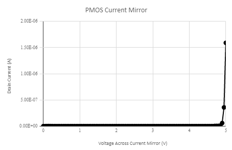
PMOS CURRENT MIRROR DATA TABLE used to create
graph above:
|
VOLTAGE
(V) |
CURRENT
(A) |
|
0 |
0 |
|
1 |
0.121 pico |
|
2 |
0.282
pico |
|
3 |
0.264 pico |
|
4 |
0.301
pico |
|
5 |
1.59 u |
NMOS CASCODE CURRENT MIRROR:
The current mirror circuit used for the NMOS consists of a PMOS
reading in the Vbiasp voltage connected to two NMOS
devices that are gate drain connected, and the drains of those NMOS devices are
cascaded into two other NMOS devices. We then inputted the variable voltage to
the rightmost NMOS and measured the drain current on that side of the current
mirror.
Below is a photo of both NMOS and PMOS cascode
current mirrors:
The NMOS version is the middle two chips and the PMOS version is
the bottom two chips.


The LTSpice simulations show the current ranging from 0 to 1.2uA
over a span of 0 to 5V.

EXPERIMENTAL
The IV curve from our experimental results shows a range of 0 to
2uA which is not as accurate as the previous measurements, but this is due to
the lack of equipment in the lab. We were forced to use two different chips to
create the cascode current mirrors, thus explaining
the lack of consistency between plots and simulations.

DATA
TABLE NMOS CASCODE CURRENT MIRROR used to create graph above:
|
VOLTAGE
(V) |
CURRENT
(A) |
|
0 |
-4.68n |
|
1 |
0.194m |
|
2 |
0.1972m |
|
3 |
0.1974m |
|
4 |
0.197m |
|
5 |
0.1974m |
PMOS CASCODE CURRENT MIRROR
The topology of the PMOS cascode current
mirror consists of an NMOS on the bottom biased with the Vbiasn
voltage, whose drain is connected to two cascoded
gate drain connected PMOS devices. The drains of these PMOS devices are fed
into the gates of the right most PMOS devices, and the variable voltage is fed
into the source of the right most PMOS. We measured the drain current of that
PMOS.

The LTSpice simulation below shows a range of current from 0 to
2uA from 0 to 5V.
 .
.
EXPERIMENTAL
Experimental IV curve shows a slight inaccuracy since the current
goes from 0 to 30mA. This is again due to the usage of two different chips to
create the cascode circuit because of a lack of
equipment in the lab.

PMOS
CASCODE CURRENT MIRROR DATA TABLE used to create the graph above.
|
VOLTAGE
(V) |
CURRENT
(A) |
|
0 |
6.81 pico |
|
1 |
0.769 pico |
|
2 |
0.682
pico |
|
3 |
0.238 pico |
|
4 |
-0.241
pico |
|
5 |
0.29 m |
Return to 420L students
Return to 420L