|
Lab 9: Design of a Beta-Multiplier Reference (BMR) - EE 420L Author: Mario Verduzco Email: Verdum1@unlv.nevada.edu Date: 04/18/17
|
|
Pre-lab:
|
|
Lab description:
|
|
Experimental results:
|
|
Conclusion:
|
|
· This lab will use the level=1 MOSFET model created in lab 8 and, again, the MOSFETs in the CD4007.pdf CMOS transistor array. · Design and simulate the operation of a BMR that biases the NMOS devices so that they have a gm of 20 uA/V à Use a simple (big) resistor to VDD for the start-up circuit (explain how the addition of a resistor ensures start-up). à When the BMR is operating the current in the big resistor should be much smaller than the current flowing in each branch of the BMR · Write-up, similar to a homework assignment, your design calculations and simulation results. (This will count as the pre-lab quiz.) · Ensure that you show the following in what you turn in: à Hand calculations à Operation as VDD is swept from 0 to 10 V * Vbiasn should stabilize (be constant) after VDD hits a minimum value (estimate this value of VDD assuming VGS/VSG is a threshold voltage and VDS,sat/ VSD,sat is zero). * Vbiasp should follow VDD after VDD hits a minimum value (show this in simulations) à Unstable operation if too much capacitance is shunting the BMR's resistor (see bottom of page 630) à Comments comparing the hand calculations with the simulation results
|
|
The objective of this lab is to use the characterized CD4007 transistor array to design, simulate, and build a beta-multiplier reference circuit that will be able to bias an NMOS and PMOS current mirror. Also using the NMOS and PMOS current mirror we will drive two gate-drain connected devices and bias a cascode current mirror. |
|
Experiment #1: Beta-Multiplier Reference |

|
1) Hand Calculations |

|
2) Simulations |

|
Vbiasp (Blue), Vbiasn (Red), and VDD (Light Blue) |
|
Current through M3 |


|
Current through M4 |
|
2) Experimental Results |

|
Experiment #2: NMOS and PMOS Current Mirrors |
|
NMOS current Mirror |


|
Current Mirror Simulation |
|
Current Mirror experimental results |

|
PMOS current Mirror |

|
Current Mirror Simulation—Current through the mirror |
|
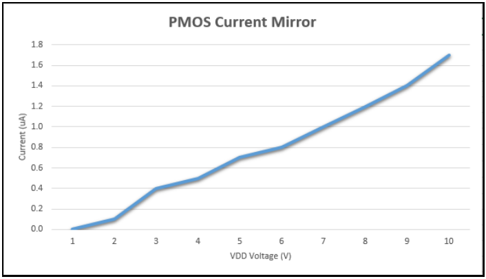
Current Mirror experimental results– Current through the mirror |
|
Experiment #3: NMOS and PMOS Cascode Current Mirrors |


|
Cascode Current Mirror Simulation |
|
Cascode Current Mirror experimental results |
|
NMOS Cascode current Mirror |
|
PMOS Cascode current Mirror |

|
Cascode Current Mirror Simulation |


|
Vbiasn stabilizes around 1v and Vbiasp follows VDD being 1v bellow VDD. |
|
Using the function generator to produce a ramp function (purple wave form) that goes from 0 to 10 v I was able to see the outputs Vbiasn (Blue) and Vbiasp (Light Blue) match closely to the simulation results. |
|
Using the Vbiasn from the beta-multiplier I was able to Bias an NMOS current mirror that was able to drive two PMOS devices that were drain-gate connected. |
|
Using the Vbiasp from the beta-multiplier I was able to Bias a PMOS current mirror that was able to drive two NMOS devices that were drain-gate connected. |
|
Using the NMOS current mirror I was able to Bias a PMOS cascode structure by using the gate voltages from the two PMOS loads. |
|
Using the PMOS current mirror I was able to Bias an NMOS cascode structure by using the gate voltages from the two NMOS loads. |
|
This lab was able to show the importance of transistor matching when trying to build a Bias voltage reference or trying to mirror any current. In order to fix this problem it is essential that the devices that are being used come from the same Wafer, Or (even better) all on the same die, because any change in the doping will cause changes in the KP of the device that will change the current through the device. |
|
An important design consideration is to add a Big resistor from the power supply to Vbiasn. This allows the Beta-multiplier to start up by injecting current into the circuit. When the BMR starts up there will be very little current through the Big resistor because the voltage across the VDD-Vbiasn divided by a huge resistance. |