|
Lab 8: Characterization of the CD4007 CMOS Transistor Array- EE 420L
Author: Mario Verduzco Email: Verdum1@unlv.nevada.edu Date: 04/05/17
|
|
Pre-lab: · Review the data sheet for the CD4007.pdf CMOS transistor array. · Ensure that you understand how the bodies of the NMOS are tied to pin 7 (VSS, generally the lowest potential in the circuit, say ground) and the bodies of the PMOS are tied to pin 14 (VDD, generally the highest potential in the circuit.
|
|
Lab description: The objective for this lab is to understand and characterize the CD4007 transistor array by creating level 1 spice models. Then we will use those models in a simulation in order to compare the models to the actual experimental results. |
|
Experimental Results: Experiment #1: Characterization of the NMOS |
|
1) ID v. VGS (0 < VGS < 3 V) with VDS = 3 V |
|
2) ID v. VDS (0 < VDS < 5 V) for VGS varying from 1 to 5 V in 1 V steps |
|
3) ID v. VGS (0 < VGS < 5 V) with VDS = 5 V for VSB varying from 0 to 3 V in 1 V steps.
|

|
Fig 1.1 – Vout (Purple) without Rbig in the feedback
|

|
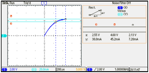
Experimental measurement: ID v. VGS (0 < VGS < 3 V) with VDS = 3 V |

|
Simulation using models: ID v. VGS (0 < VGS < 3 V) with VDS = 3 V |
|
Fig 1.1 – Vout (Purple) without Rbig in the feedback
|

|
Experimental measurements: |
|
ID v. VDS (0 < VDS < 5 V) for VGS =1v |

|
ID v. VDS (0 < VDS < 5 V) for VGS =2v |

|
ID v. VDS (0 < VDS < 5 V) for VGS =3v |
|
ID v. VDS (0 < VDS < 5 V) for VGS =4v |


|
ID v. VDS (0 < VDS < 5 V) for VGS =5v |

|
Simulation using models: ID v. VDS (0 < VDS < 5 V) for VGS varying from 1 to 5 V in 1 V steps |


|
Experimental measurements: |
|
ID v. VGS (0 < VGS < 5 V) with VDS = 5V VSB = 0 |

|
ID v. VGS (0 < VGS < 5 V) with VDS = 5V VSB = 1 |
|
ID v. VGS (0 < VGS < 5 V) with VDS = 5V VSB = 2 |
|
ID v. VGS (0 < VGS < 5 V) with VDS = 5V VSB = 3 |


|
Simulation using models: ID v. VGS (0 < VGS < 5 V) with VDS = 5 V for VSB varying from 0 to 3 V in 1 V steps. |

|
4) Determining level=1 Spice parameters
|

|
5) Summary of Results
|

|
1) ID v. VG (0 < VG < 3 V) with VSD = 3 V |
|
2) ID v. VSD (0 < VDS < 5 V) for VG varying from 1 to 5 V in 1 V steps |
|
Experimental measurement: ID v. VG (0 < VGS < 3 V) with VS = 3 V |
|
Simulation using models: ID v. VG (0 < VGS < 3 V) with VSD = 3 V |
|
Experimental measurements: |
|
ID v. VSD (0 < VDS < 5 V) for VG =1v |
|
ID v. VSD (0 < VDS < 5 V) for VG =2v |
|
ID v. VSD (0 < VDS < 5 V) for VG =3v |
|
ID v. VSD (0 < VDS < 5 V) for VG =4v |
|
ID v. VSD (0 < VDS < 5 V) for VG =5v |
|
Simulation using models: ID v. VSD (0 < VDS < 5 V) for VG varying from 1 to 5 V in 1 V steps |
|
Experimental measurements: |
|
ID v. VG (0 < VGS < 5 V) with VSD = 5V VB = 5v |
|
ID v. VG (0 < VGS < 5 V) with VSD = 5V VB = 6v |
|
ID v. VGS (0 < VG < 5 V) with VSD = 5V VB = 7v |
|
ID v. VGS (0 < VS < 5 V) with VSD = 5V VB = 8v |
|
Simulation using models: ID v. VG (0 < VG < 5 V) with VSD= 5 V for VBS varying from 0 to 3 V in 1 V steps. |
|
4) Determining level=1 Spice parameters
|
|
5) Summary of Results
|

|
Experiment #1: Characterization of the PMOS
|


|
3) ID v. VG (0 < VG < 5 V) with VSD = 5 V for VB varying from 0 to 3 V in 1 V steps |


|
Experiment #3 Characterization of the CMOS inverter
|


|
Simulation using models: Delay |
|
Experimental measurement: Delay |
|
Spice Parameter |
Value |
|
W/L |
100 |
|
Cox |
5pF |
|
C’ox |
2fF/um^2 |
|
T’ox |
17.25nm |
|
Vthn |
1.55v |
|
KPn |
147uA/V^2 |
|
Lambda |
0.028V^-1 |
|
Gamma |
0.288V^1/2 |
|
Spice Parameter |
Value |
|
W/L |
100 |
|
Cox |
5pF |
|
C’ox |
2fF/um^2 |
|
T’ox |
17.25nm |
|
Vthn |
1.11v |
|
KPn |
54.3uA/V^2 |
|
Lambda |
0.089V^-1 |
|
Gamma |
0.288V^1/2 |