|
Lab 6: Single stage transistor amplifiers - EE 420L
Author: Mario Verduzco Email: Verdum1@unlv.nevada.edu Date: 03/08/17
|
|
Pre-lab: · This lab will utilize the ZVN3306A and ZVP3306A MOSFETs. · Review these datasheets and become familiar with these transistors. · Verify that the simulations seen in lab6_sims.zip reasonably model the behavior of the transistors' ID v. VGS, ID v. VDS, and gm v. VGS curves. · Finally, watch the video single_stage_amps and review single_stage_amps.pdf |
|
Lab description: The objective of this lab is to evaluate, simulate, and build a source follower, common gate, common source, and push-pull amplifier using both NMOS and PMOS topologies. Also, to measure their respective gain, input and output resistances. |
|
Experimental Results: Experiment #1: NMOS and PMOS Source Follower Amplifier |
|
1) Simulation results |
|
2) Hand Calculations |
|
3) Experimental Results
|


|
NMOS: Gain=1 |

|
PMOS: Gain=1 |
|
Fig 1.1 – NMOS source follower simulation
|
|
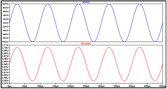
Fig 1.2– PMOS source follower simulation
|


|
NMOS: Gain=1 |
|
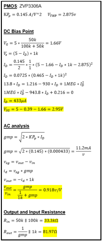
PMOS: Gain=1.09 |
|
4) Determining Input and Output resistance |
|
Fig 1.3 – NMOS source follower gain Vin(Blue) Vout(Teal)
|
|
Fig 1.4 – PMOS source follower gain Vin(Blue) Vout(Teal)
|

|
NMOS Input resistance using a 33kohm resistor |

|
NMOS output resistance using a 51ohm resistor |

|
PMOS Input resistance using a 33kohm resistor |
|
PMOS output resistance using a 80ohm resistor |
|
Fig 1.5 – NMOS source follower Input resistance Vin(Blue) Vout(Teal)
|
|
Fig 1.7 – NMOS source follower Output resistance Vin(Blue) Vout(Teal)
|
|
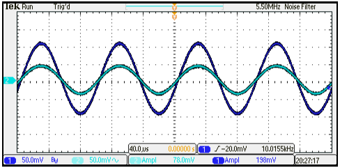
Fig 1.6 – PMOS source follower Input resistance Vin(Blue) Vout(Teal)
|
|
Fig 1.8 – PMOS source follower Output resistance Vin(Blue) Vout(Teal)
|
|
5) Summary of results |
|
Experiment #2: NMOS and PMOS Common Source Amplifier |

|
1) Simulation results |


|
NMOS: Gain=-7 |
|
PMOS: Gain=-5.5 |
|
Fig 1.9 – NMOS Common Source simulation
|
|
Fig 1.10– PMOS Common Source simulation
|
|
2) Hand Calculations |


|
3) Experimental Results
|

|
NMOS: Gain=-5.46 |

|
PMOS: Gain=-3.1 |
|
Fig 1.11 – NMOS Common Source gain Vin(Blue) Vout(Teal)
|
|
Fig 1.12– PMOS Common Source gain Vin(Blue) Vout(Teal)
|
|
4) Determining Input and Output resistance |

|
NMOS Input resistance using a 33kohm resistor |
|
Fig 1.13– NMOS Common Source Input resistance Vin(Blue) Vout(Teal)
|

|
NMOS output resistance using a 1kohm resistor |
|
Fig 1.15 – NMOS Common Source Output resistance Vin(Blue) Vout(Teal)
|


|
PMOS Input resistance using a 33kohm resistor |
|
PMOS output resistance using a 1kohm resistor |
|
Fig 1.14– PMOS Common Source Input resistance Vin(Blue) Vout(Teal)
|
|
Fig 1.16 – PMOS Common Source Output resistance Vin(Blue) Vout(Teal)
|
|
5) Summary of results |
|
Experiment #3: NMOS and PMOS Common Gate Amplifier |

|
1) Simulation results |
|
NMOS: Gain=6 |

|
PMOS: Gain=5 |
|
Fig 1.17 – NMOS Common Gate simulation
|
|
Fig 1.18– PMOS Common Gate simulation
|
|
2) Hand Calculations |


|
3) Experimental Results
|


|
NMOS: Gain=4.89 |
|
PMOS: Gain=2.65 |
|
Fig 1.19– NMOS Common gate gain Vin(Blue) Vout(Teal)
|
|
Fig 1.20– PMOS Common gate gain Vin(Blue) Vout(Teal)
|
|
4) Determining Input and Output resistance |


|
NMOS Input resistance using a 152ohm resistor |
|
NMOS output resistance using a 1kohm resistor |
|
PMOS Input resistance using a 182ohm resistor |
|
PMOS output resistance using a 1kohm resistor |
|
Fig 1.21– NMOS Common Gate Input resistance Vin(Blue) Vout(Teal)
|
|
Fig 1.22– PMOS Common Gate Input resistance Vin(Blue) Vout(Teal)
|
|
Fig 1.23 – NMOS Common Gate Output resistance Vin(Blue) Vout(Teal)
|
|
Fig 1.24– PMOS Common Gate Output resistance Vin(Blue) Vout(Teal)
|
|
5) Summary of results |
|
Experiment #4: Push Pull amplifier |

|
1) Simulation results |

|
Push Pull with 100k: Gain=2k |

|
Push Pull with 510k: Gain=2.5k |
|
2) Hand Calculations |
|
Fig 1.25 – Push Pull amplifier with 100k resistor simulation
|
|
Fig 1.26– Push Pull amplifier with 510k resistor simulation
|

|
3) Experimental Results
|


|
Push Pull with 100k: Gain= 1700 |
|
Push Pull with 510k: Gain= 2600 |
|
Fig 1.27 – Push Pull amplifier with 100k resistor
|
|
Fig 1.28– Push Pull amplifier with 510k resistor
|

|
Push Pull Vin after voltage dividor |
|
Fig 1.28– Push Pull amplifier Vin
|
|
5) Summary of results |
|
The Source follower amplifier (Common Drain amplifier) is an amplifier with the Vin and Vout having a common node at the drain of the MOSFET. This amplifier is Biased with a voltage dividor on the VDD. This is a non inverting amplifier with a large input resistance. The amplifier has a very small gain of approximately 1.
When Using electrolytic capacitors it is important to follow the DC voltage. For example in the NMOS topology the positive side of the capacitor should be on the 3.33v Bias and the negative should be facing toward the Vin because there is only an AC voltage on Vin and no DC voltage. |
|
In order to determine the Input and Output resistance one can add a resistor in series with either the input or output of the same value as the calculated Input/Output resistance. This will form a voltage divider making the vout or vin be halved. When measuring the Output resistance it is important to add a large capacitor in order not to mess up the Bias voltage. |
|
The Common Source Amplifier is an amplifier with the Vin and Vout Common at the Source of the MOSFET. This amplifier has a High Input resistance and a high AC voltage Gain. This amplifier also has a high Output resistance. Again this amplifier is Biased using a voltage divider on VDD. |
|
NMOS Value |
Simulation |
Hand Calculation |
Experimental |
|
Gain |
1 |
0.948 |
1 |
|
Rin |
33.33k |
33.33k |
33k |
|
Rout |
51.8 |
-51.8 |
52 |
|
PMOS Value |
Simulation |
Hand Calculation |
Experimental |
|
Gain |
1 |
0.918 |
1.09 |
|
Rin |
33.33k |
33.33k |
33k |
|
Rout |
82 |
82 |
80 |
|
NMOS Value |
Simulation |
Hand Calculation |
Experimental |
|
Gain |
-7 |
-6.87 |
-5.46 |
|
Rin |
33.33k |
33.33k |
33k |
|
Rout |
1k |
1k |
1k |
|
PMOS Value |
Simulation |
Hand Calculation |
Experimental |
|
Gain |
-5.5 |
-5.55 |
-3.1 |
|
Rin |
33.33k |
33.33k |
33kj |
|
Rout |
1k |
1k |
1k |
|
NMOS Value |
Simulation |
Hand Calculation |
Experimental |
|
Gain |
6 |
6.33 |
4.89 |
|
Rin |
151.8 |
151.8 |
152 |
|
Rout |
1k |
1k |
1k |
|
PMOS Value |
Simulation |
Hand Calculation |
Experimental |
|
Gain |
5 |
5.04 |
2.65 |
|
Rin |
182 |
182 |
182 |
|
Rout |
1k |
1k |
1k |
|
NMOS Value |
Simulation |
Hand Calculation |
Experimental |
|
Gain 100k |
-2k |
-2.5k |
-1700 |
|
Gain 510k |
-2.5k |
-15k |
-2600 |