|
Lab 3: Op-amps I, basic topologies, finite gain, offset- EE 420L
Author: Mario Verduzco Email: Verdum1@unlv.nevada.edu Date: 02/14/17
|
|
Pre-lab: · Watch the video op_amps_I, review op_amps_I.pdf (associated notes), and simulate the circuits in op_amps_I.zip. · Read the write-up seen below before coming to lab. |
|
Lab description: The objective for this lab is to understand the non-inverting, and inverting topologies for an op-amp. Also, to understand that non ideal op-amps have finite gain and offsets. |
|
Experimental Results: Experiment #1: Building and testing the following Op-Amp circuit |
|
Experiment #2: Measuring Op-Amp offset voltage |
|
Fig 1.4 – Common-mode voltage VCM |
|
Fig 1.5 – Vout without DC offset on Oscope
|
|
Fig 1.6 – Vout With DC offset
|

|
1) What is the common-mode voltage, VCM? Does VCM change? Why or why not? |

|
The VCM is the voltage seen by both inverting and noninverting inputs of the Op-Amp. Vcm remains constant at 2.5v. It does not change because the power supply is applying a constant 5v across a voltage divider keeping Vcm at 2.5v |
|
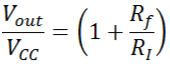
2) What is the ideal closed-loop gain? |


|
3) What is the output swing and what is it centered around? -What happens if the input isn't centered around VCM, that is, 2.5 V? -Provide a detailed discussion illustrating that you understand what is going on. |


|
The Vout of the Op-Amp shows a 1kHz sine wave with a Vpp of 100mV with a DC offset of 2.5v. When the input was not centered around 2.5v the sine wave was centered at 5v but the upper half was clipped. This occurs because the Op-Amp is only being powered to +5v therefore the sine wave cannot exceed +5v. Also, the 2.5v DC appears at the output as –2.5v because of the fain of –1, so this –2.5v subtracts from the +5v seen at the output from the VCC. |
|
4) What is the maximum allowable input signal amplitude? Why? |
|
The maximum allowable input signal amplitude with a DC offset of 2.5v is a little under 5vpp, Because the Op-Amp only has a gain of -1 and is operating on rails of 0v to +5v so a signal centered at 2.5v DC can go up to a little before the power supply rails. |
|
5) What is the maximum allowable input signal if the magnitude of the gain is increased to 10? Why? |
|
The maximum allowable input signal amplitude with a DC offset of 2.5v and a gain of 10 would be a signal with a max amplitude a little less than 250mV because the Op-Amp will amplify the 250mV to 2.5v which will reach the top and bottom rails of the Op-Amps power supply. |
|
6) What is the point of the 0.01 uF capacitors from VCC and VCM to ground? -Are these values critical or could 0.1 uF, 1,000 pF, 1 uF, etc. capacitors be used? |
|
The 0.01 uF capacitors act as decoupling capacitors and are used to provide a constant DC voltage to VCM because power supply is not ideal so the capacitor will hold charge keeping the voltage on that node. These values are not critical and any capacitance can be used given that the start up time does not matter. |
|
7) The data sheet shows that this op-amp has an input bias current that flows out of the op-amp's inputs of typically 20 nA. -This current flows out of both the non-inverting and inverting inputs through the resistors connected to these inputs.
-Show how the operation of the circuit can be effected if, for example, R1 and R2, are much larger. Ex plain what is going on. *What is the input offset current? What does this term describe? |
|
When there is an input offset current flowing through the non-inverting input there will be a voltage drop across the R1 and R2 resistors. If these resistors are very large then the voltage drop across them will be very high which will in turn change the Vcm. |

|
1) Explain how the following circuit can be used to measure the op-amp’s offset voltage. -To measure small offset voltages increase the gain by increasing RF to 100k or larger. Explain what is going on. |
|
The offset of the Op-Amp can be measured here because the voltage drop across R4 is Vcm-Vm and that current will also go through R3 and using that you can measure the Vout by measuring the voltage drop across R3. If a 1ook resistor is used then the voltage seen on Vout will be 100 times larger. |
|
2) Measure the offset voltage of 4 different op-amps and compare them.
|
|
Using the topology above I measured the offset voltages of 4 different Op-Amps. |

|
Fig 1.7 – LM 324 Offset voltage
|

|
Fig 1.9 – LM 339 Offset voltage
|
|
Fig 1.10 – LM 339 Offset voltage from Datasheet
|

|
LM 324 |
|
LM 339 |
|
TL081 |
|
Fig 1.11 – TL081 Offset voltage
|
|
Fig 1.12 – TL081 Offset voltage from Datasheet
|

|
Ua741 |
|
Fig 1.13 – Ua741 Offset voltage
|
|
Fig 1.14 – Ua741 Offset voltage
|
|
Lab Questions: 1) Knowing the non-inverting input, Vp, is at the same potential as the inverting input, Vm, (called the common-mode voltage, VCM) what are the maximum and minimum allowable common-mode voltages?
|

|
As seen below in the data sheet the Max Vcm=Vcc-1.5v so in our case Vcm = 5v-1.5v = 3.5v. The minimum Vcm = 0v. |
|
2) What is a good estimate for the op-amp's open-loop gain?
|
|
The Open-loop gain can be found using the open-loop frequency response graph found in the data sheet. From the graph we can see that with a 1kHz signal we see an AoL of 55dB which equals a gain of 562.3v/V. |

|
Fig 1.1 – Vicm from datasheet |
|
3) What is a good estimate for the offset voltage?
|
|
Fig 1.2 – Open loop frequency response from datasheet |


|
Fig 1.8 – LM 324 Offset voltage from Datasheet
|
|
Fig 1.3 – LM 324 Offset voltage from Datasheet
|
|
A good estimate for the offset voltage is 2mV which can be found in the typical value column from the Op-Amp Datasheet. However when designing for worst case scenario I would design with a 9mV offset in mind. |
|
Op Amp |
Measured Offset voltage |
|
LM324 |
0.3mV |
|
LM339 |
0.01mV |
|
TL081 |
9.6mV |
|
Ua741 |
1.4mV |