Lab 9 - ECE 420L 

Authored by Stephanie Silic

silics@unlv.nevada.edu

April 19th, 2017


Lab Description


In this lab we are going to use the Spice MOSFET models we created from experimental data in Lab 8 and design a BMR that biases the NMOS devices so that they have a gm of 20uA/V.


Lab Report


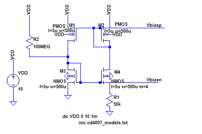
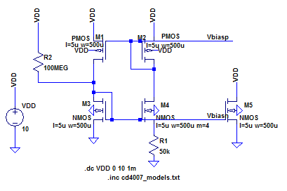
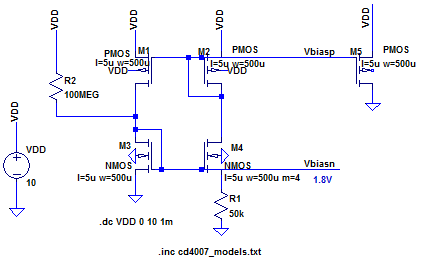
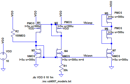
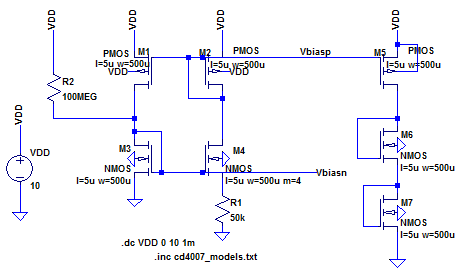
The BMR circuit is the following:

 
 http://cmosedu.com/jbaker/courses/ee420L/s17/students/silics/Lab9/schematic_BMR.PNG        
 
The resistor value is chosen based on the following reasoning:
 
http://cmosedu.com/jbaker/courses/ee420L/s17/students/silics/Lab9/calcs.PNG    
 
Here, the KP values had been changed to even lower values than presented at the end of Lab 8. This was done to better match the current measured in the actual BMR circit. I continued to try to match the the results with the simulations throughout this lab. The initial hand calculation above shows the thought process, the actual values attained for Id and the KPs used turned out to be incorrect. The reasoning for the 50k value of R remains sound, however.

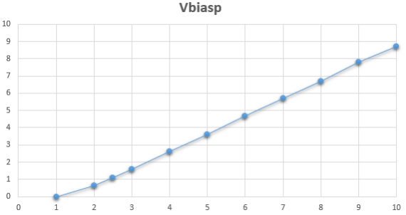
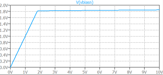
After building this circuit with the CD4007 chips on the breadboard I measured the voltage at the gate of M3 (of the spice schematic) for Vbiasn, the gate of M2 for the Vbiasp voltage, and the voltage across the resistor to measure the current Iref. 
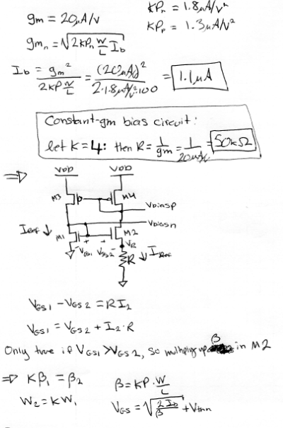
We expect Vbiasn to maintain a fairly constant value after the threshold voltage of 2V, though it will increase with VDD. We expect Vbiasp to increase linearly with VDD, and we expect Iref to be at least 1.1uA (based on the initial calculations above), again after the higher threshold voltage, around 2V.


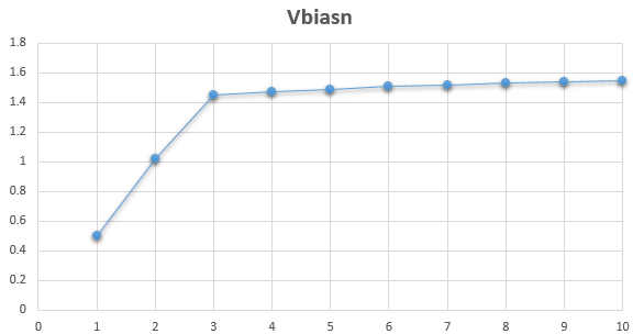
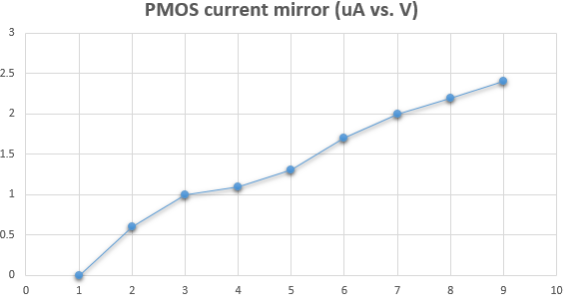
Table and plots of experimental values from BMR circuit are shown below, followed by the simulations generated by the Spice models:


http://cmosedu.com/jbaker/courses/ee420L/s17/students/silics/Lab9/table_BMR_ckt.PNG   


http://cmosedu.com/jbaker/courses/ee420L/s17/students/silics/Lab9/plot_Vbiasn.PNG http://cmosedu.com/jbaker/courses/ee420L/s17/students/silics/Lab9/plot_Vbiasp.PNG http://cmosedu.com/jbaker/courses/ee420L/s17/students/silics/Lab9/plot_IREF.PNG


  http://cmosedu.com/jbaker/courses/ee420L/s17/students/silics/Lab9/sim_Vbiasn.PNG http://cmosedu.com/jbaker/courses/ee420L/s17/students/silics/Lab9/sim_Vbiasp.PNG http://cmosedu.com/jbaker/courses/ee420L/s17/students/silics/Lab9/Sim_Iref_1.PNG


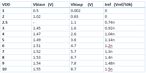
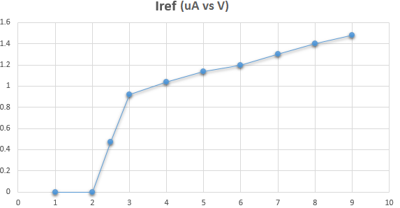
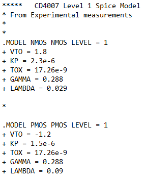
The BMR seems to be started up at nearly 3V VDD, and teh Iref simulation is a lot lower than the measured values (and expectations). Adjusting the KPn in the Spice model to a higher value gives us the following Iref:


http://cmosedu.com/jbaker/courses/ee420L/s17/students/silics/Lab9/Sim_Iref_2.PNG


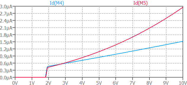
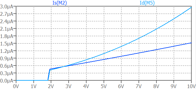
The Spice models now as follows:


http://cmosedu.com/jbaker/courses/ee420L/s17/students/silics/Lab9/spice_model.PNG


The NMOS and PMOS current mirrors:


     http://cmosedu.com/jbaker/courses/ee420L/s17/students/silics/Lab9/schematic_NMOS_mirror.PNG  http://cmosedu.com/jbaker/courses/ee420L/s17/students/silics/Lab9/schematic_PMOS_mirror.PNG


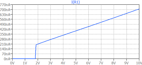
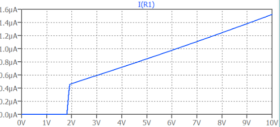
To measure the current experimentally through the NMOS and PMOS devices in the current mirrors, an ammeter was placed in series with the devices, and the readings plotted versus VDD varying from 0 to 10V:


http://cmosedu.com/jbaker/courses/ee420L/s17/students/silics/Lab9/Table_NMOS_mirror.PNG                                               http://cmosedu.com/jbaker/courses/ee420L/s17/students/silics/Lab9/table_PMOS_mirror.PNG


http://cmosedu.com/jbaker/courses/ee420L/s17/students/silics/Lab9/plot_NMOS_mirror.PNG   http://cmosedu.com/jbaker/courses/ee420L/s17/students/silics/Lab9/plot_PMOS_mirror.PNG


   http://cmosedu.com/jbaker/courses/ee420L/s17/students/silics/Lab9/sim_NMOS_mirror.PNG     http://cmosedu.com/jbaker/courses/ee420L/s17/students/silics/Lab9/sim_PMOS_mirror.PNG


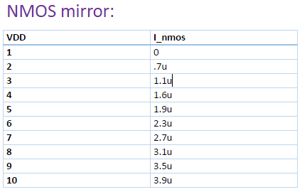
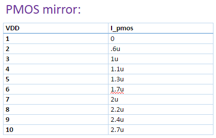
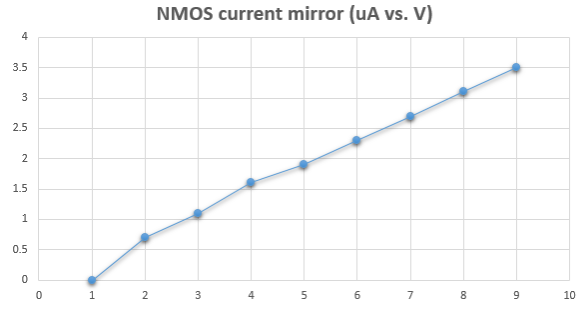
We expect, as we see in the above results, that the bias voltages will increase with increasing VDD. But the variation of the measured data seems to vary far too much; the simulations vary less, and I did not deem it necessary to try to match the simulations once more to the data this time. Either something is wrong in the circuit or how I measured the voltage, or the BMR is simply not that good. The BMR is not designed to be a stable reference with respect to VDD, so this is the reason accepted as to why the Vbiasn is increasing so linearly with VDD.


NMOS current mirror driving two gate-drain connected PMOS devices and a PMOS current mirror driving two gate-drain connected NMOS devices:


  http://cmosedu.com/jbaker/courses/ee420L/s17/students/silics/Lab9/schematic_NMOS_driving.PNG  http://cmosedu.com/jbaker/courses/ee420L/s17/students/silics/Lab9/schematic_PMOS_driving.PNG


http://cmosedu.com/jbaker/courses/ee420L/s17/students/silics/Lab9/table_NMOS_cas.PNG  http://cmosedu.com/jbaker/courses/ee420L/s17/students/silics/Lab9/table_PMOS_cas.PNG


      http://cmosedu.com/jbaker/courses/ee420L/s17/students/silics/Lab9/plot_NMOS_casPNG.PNG   http://cmosedu.com/jbaker/courses/ee420L/s17/students/silics/Lab9/plot_PMOS_casPNG.PNG

      http://cmosedu.com/jbaker/courses/ee420L/s17/students/silics/Lab9/sim_NMOS_driving_PMOSes.PNG  http://cmosedu.com/jbaker/courses/ee420L/s17/students/silics/Lab9/sim_PMOS_driving_nmos.PNG


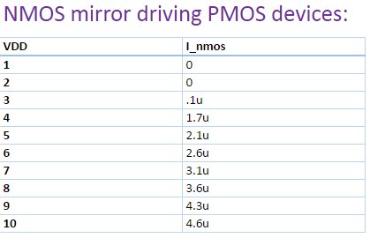
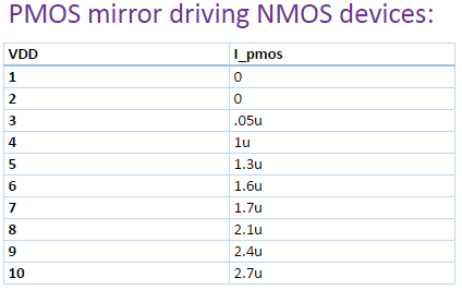
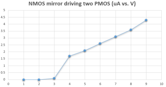
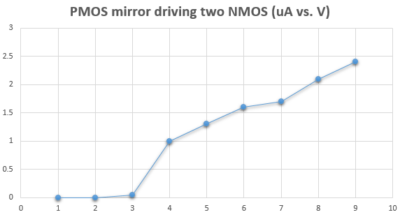
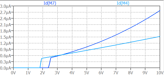
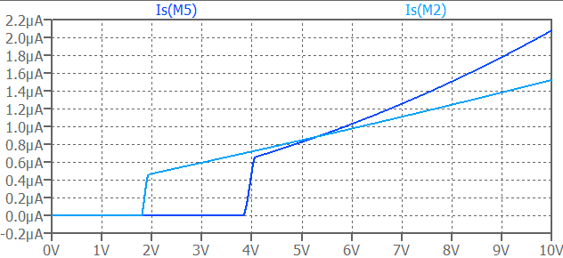
The NMOS driving two gate-drain connected PMOS devices gives a higher current in the mirror than just the NMOS mirror in the measured data. However, the simulation shows the more ideal situation, where the mirrored current with the PMOS divices added is still the same as the mirrored current with a single NMOS device. The threshold voltage has also increased by nearly a volt for the NMOS mirror and nearly two volts for the PMOS mirror, even in the simulations.


Conclusion:


Dealing with these transistors was more difficult than expected. When the results aren't what I expected, a lot of time was spent trying to troubleshoot the circuit, wondering if there was a mistake somewhere. The lessons learned from Lab 8, characterizing the MOSFETs, and this lab, creating a beta-multiplier reference have been a good introduction to real-world design, where the models don't always match the measurements, and the measurements sometimes don't match the calculations. All these things need to be balanced, and an iterative process performed: calculate, simulate, measure, and repeat. 


Return to my labs