Lab 8 - ECE 420L
Authored
by Stephanie Silic
silics@unlv.nevada.edu
April 5th, 2017
Lab Description
Characterization of the CD4007 CMOS transistor array
This
lab will show the characterization of the transistors in the CD4007
chip and how to generate SPICE Level 1 models from experimental
results. We assume that the MOSFETs will be used in the design of
circuits powered by a single +5V power supply. In other words, don't
characterize the devices at higher than +5 voltages or lower than
ground potential.
Part 1 in this lab report will be the N-channel MOSFET
characterization, Part 2 will be the P-channel MOSFET characterization,
and Part 3 will be the analysis of the CMOS inverter using this CD4007
array.
For each device, this report will include the experimentally generated plots of:
- ID v. VGS (0 < VGS < 3 V) with VDS = 3 V
- ID v. VDS (0 < VDS < 5 V) for VGS varying from 1 to 5 V in 1 V steps, and
- ID v. VGS (0 < VGS < 5 V) with VDS = 5 V for VSB varying from 0 to 3 V in 1 V steps.
and the Spice simulations using the model developed from the experiments.
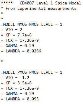
Our Model 1 Spice model of these transistors will include only VTO, KP, LAMBDA, GAMMA, and TOX.
Lab Report
Part 1: N-channel MOSFET characterization
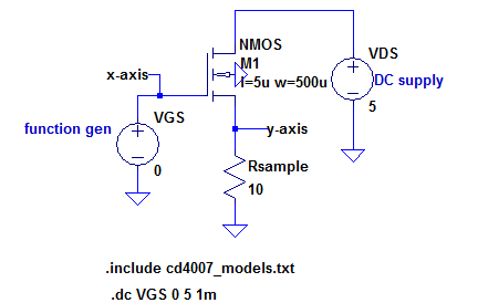
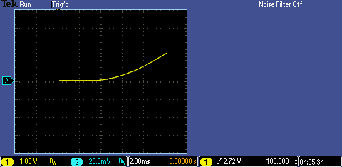
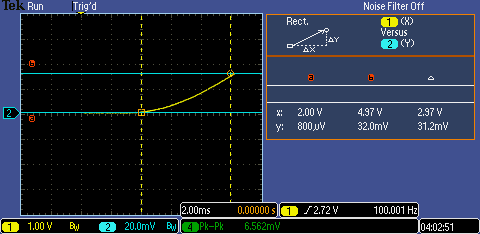
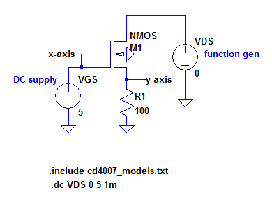
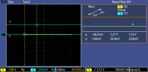
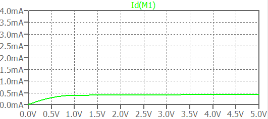
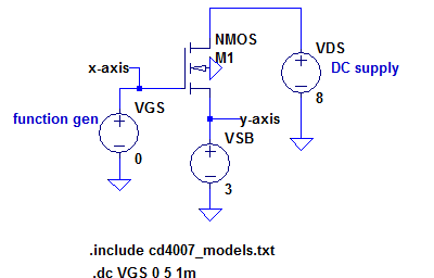
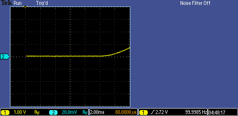
1. ID v. VGS, VGS varies from 0 to 3V, VDS = 3V
To generate the ID vs. VGS plot, VGS is connected to the function
generator with a waveform that varies from 0 to 3V, while VDS is set to
3V. A sampling resistor of 10 Ohms is placed in series with the source
of the MOSFET to ground, providing a way to know the current ID through
the device. An X-Y plot on the oscilloscope is used to view the ID vs.
VGS plot, where the X-axis is the varying VGS and the Y-axis is the
voltage across the sampling resistor. Thus, whatever value we see on
the Y-axis we devide by 10 Ohms to get the current. This resistor
should be small; 10 Ohms was chosed because it eases the numerical
calculation.
ID v. VGS circuit and plot:
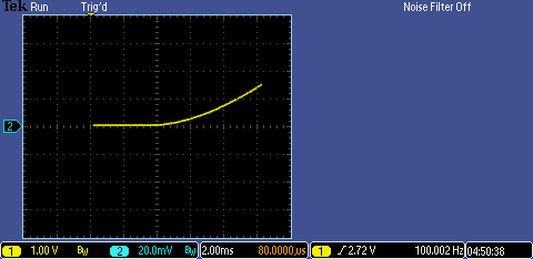
Now,
the threshold voltage for the NMOS appears to be nearly 2 V. This seems
high, especially compared to the PMOS threshold voltage, see below. A
brief discussion of the possible reasons for this will be presented
after the spice model calculations, in Part 3 of this report.
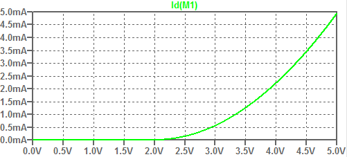
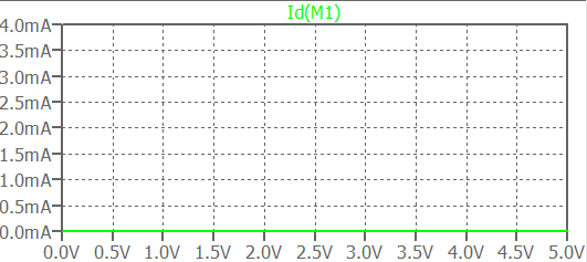
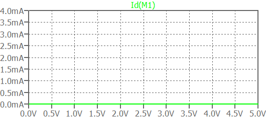
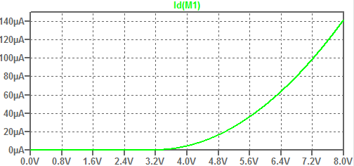
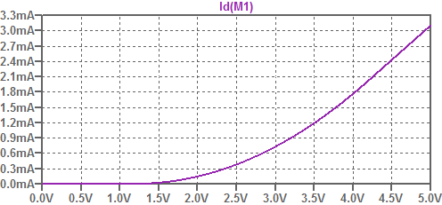
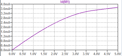
ID v. VGS plot from SPICE level 1 model (spice model discussed in Part 3):
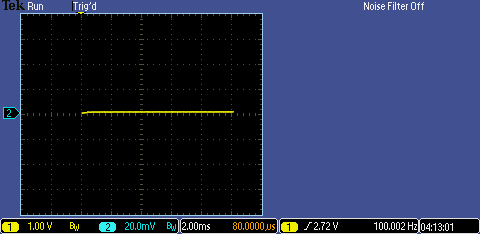
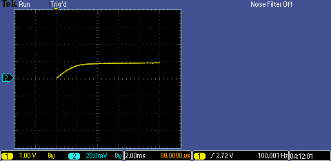
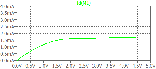
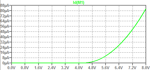
2. ID v. VDS, VDS varies from 0 to 5V, VGS values from 1 to 5V in 1V steps
For
the ID v. VDS curves, VDS was varied, while VGS was held at a constant
1, 2, 3, 4 and 5 Volts.
The
curves to the right are from the Spice model simulations of the circuit shown:
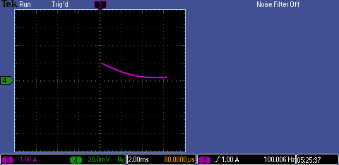
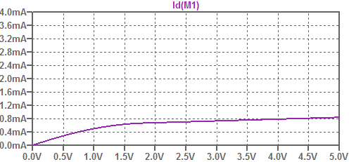
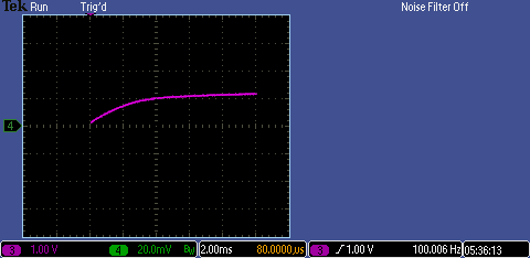
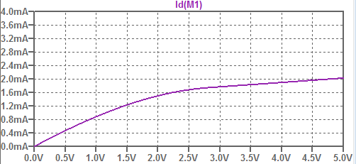
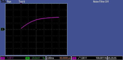
Important Note: since a 10 Ohm sampling resistor was used to measure the current, a reading of 20mV on the y-axis is 2mA, since it is 20mV/10 Ohms.
VGS = 1:
VGS = 2:
VGS = 3:
VGS = 4:
VGS = 5:
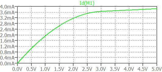
3.
ID v. VGS, VGS varies from 0 to 5V, VDS = 5V, and VSB changes from 0 to
3V in 1V steps. In the measurement circuit, the 10-ohm sampling
resistor was placed between the source and the VSB voltage.
VSB = 0V:
VSB = 1V:
VSB = 2V:
VSB = 3V:
These
simulations are pretty far off. Since all we are dealing with here is
the threshold voltage, though, it is simply important to keep in
mind that VGS must go up if the body of the MOSFET is above ground.
Part 2: P-channel MOSFET characterization
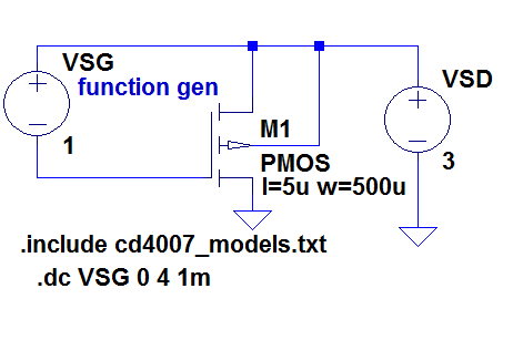
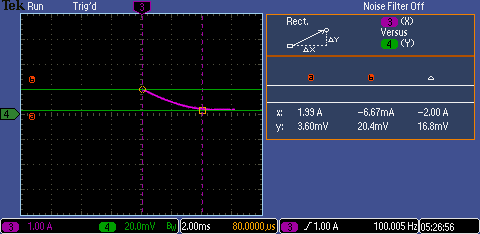
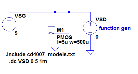
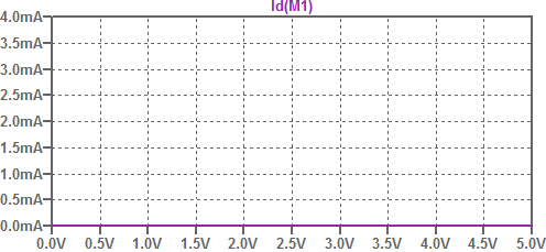
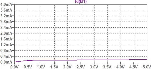
1. ID v. VSG, VSG varies from 0 to 4V.
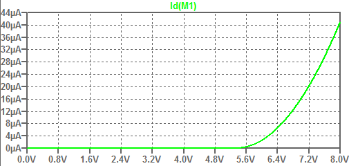
2. ID v. VDS, VDS varies from 0 to 5V, VGS values from 1 to 5V in 1V steps
Again, since a 10 Ohm sampling resistor was used to measure the current, a reading of 20mV on the y-axis is 2mA, since it is 20mV/10 Ohms.
VSG = 1V:
VSG = 2V:
VSG = 3V:
VSG = 4V:
VSG = 5V:
The
last to drain current simulations match well, while the simulations of
the ID curve at VSG = 4V is a bit low. It is harder to tell with VSG
lower than 4V.
3. ID v. VGS, VGS varies from 0 to 5V, VDS = 5V, and VSB changes from 0 to 3V in 1V steps.
This part of the lab I was unable to complete properly in time, but it does not have an affect on the spice model parameters.
Part 3: SPICE model
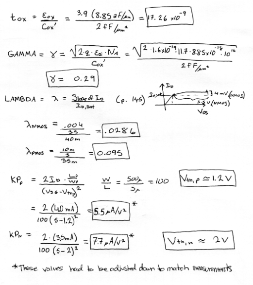
To find the parameters that will be included in our spice model, we do the following:
For TOX:
First, we are assuming the lengths and widths of the devices are 5u and 500u, respectively, or W/L is 500u/5u, and Cox is 5 pF.
Therefore, Cox' can be calculated to be 2fF/um^2
For the VTO:
We look at the experimentally generated plots and make an estimate for the threshold value.
For KP:
We solve the ID square-law equation by plugging in W/L, VGS, and ID at that VGS. (from the experimental plots)
For GAMMA:
We can find the equation for gamma on page 139 of the CMOS book. This number will be the same for both NMOS and PMOS
For LAMBDA:
Lambda
is the channel length modulation parameter. On page 145, lambda is
defined as the slope of the ID curve in saturation divided by ID,sat.
My calculations are shown below:
Again,
the threshold for the PMOS is usually greater than the threshold
voltage for the NMOS. Experimental and human error can be blamed for
this. Without totally throwing out the results seen on the oscilloscope
as false, examining how high the current in the ID vs. VGS curve when
VGS is at 5V was instructive: in the experiment that current was a
lot lower than the simulation ended up being. This justifies a lower
threshold voltage actually than what appears to be 2V on the
oscilloscope. Or, perhaps some other human error caused the discrepancy.
As
noted, the KPp value was adjusted down to make a better match with the
measured results. The models won't be perfect, but this lab has
shown how some of the most fundamental parameters can be experimentally
determined.
Spice Model after adjusting KPp to a lower value:
Return to my labs