Lab 8 - ECE 420L Engineering Electronics II Lab
Authored
by Frank Sanchez,
sanchezf@unlv.nevada.edu
4/5/2017
++++++++++++++
Experiment 1
++++++++++++++
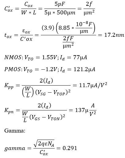
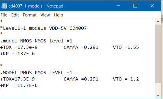
Calculated Values for DC4007 Level=1 model are below.These calculations were obtained through experimentation.
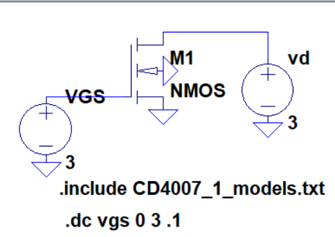
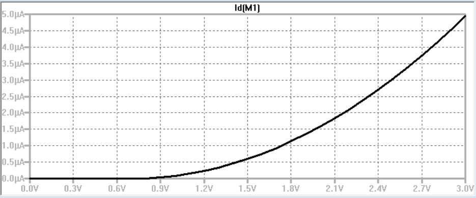
ID v. VGS (0 < VGS < 3 V) with VDS = 3 V
NMOS:
LTSPICE & Experimental Result:
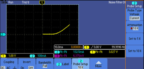
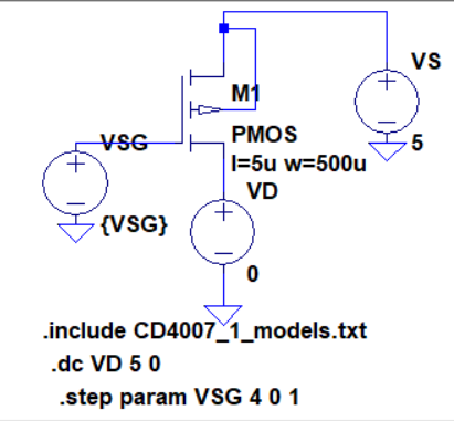
PMOS:
LTSPICE & Experimental Result:
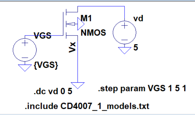
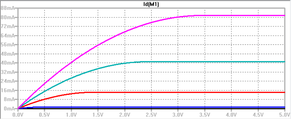
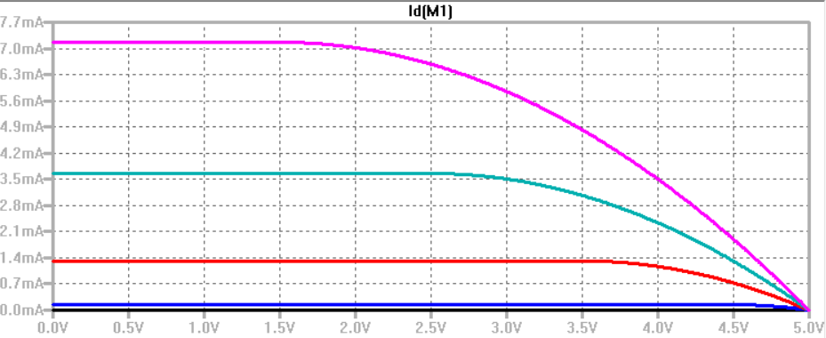
ID v. VDS (0 < VDS < 5 V) for VGS varying from 1 to 5 V in 1 V steps.
NMOS:
LTSPICE:
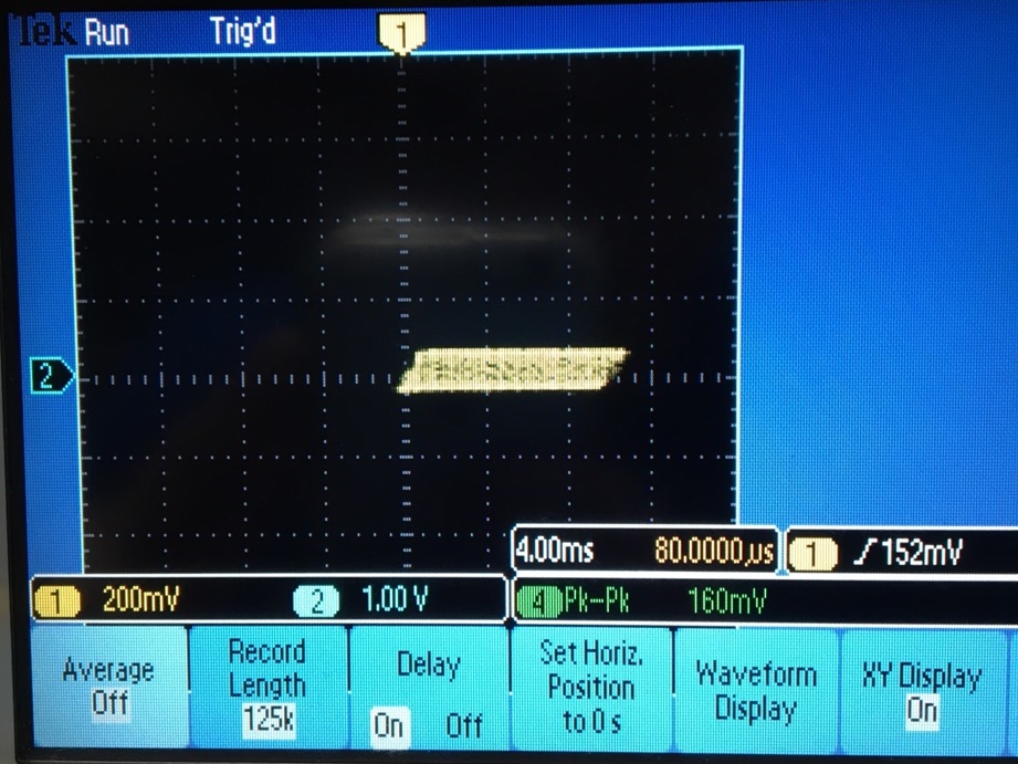
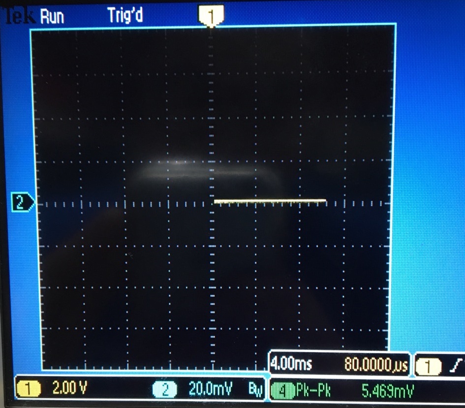
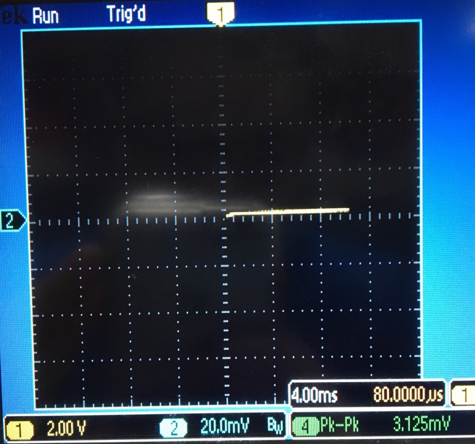
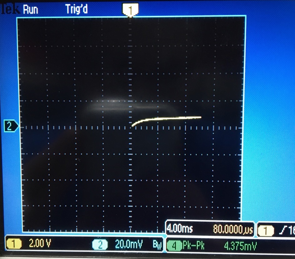
Experimental Result:
.
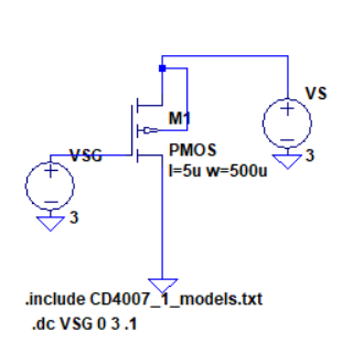
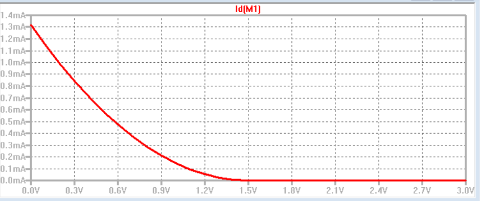
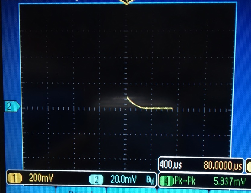
PMOS:
LTSPICE:
Experimental Result:
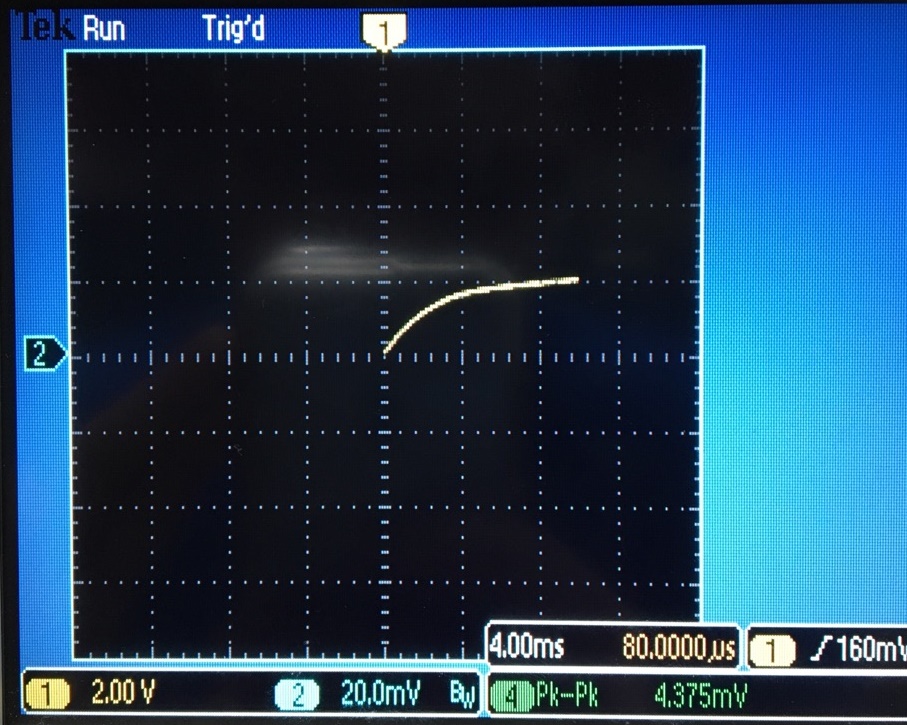
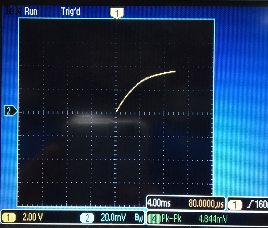
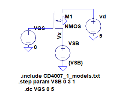
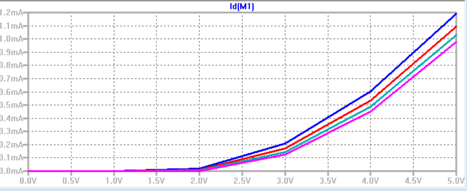
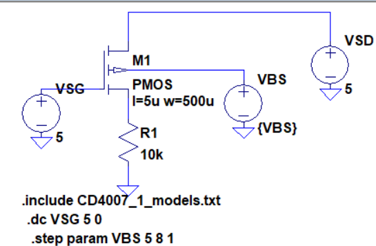
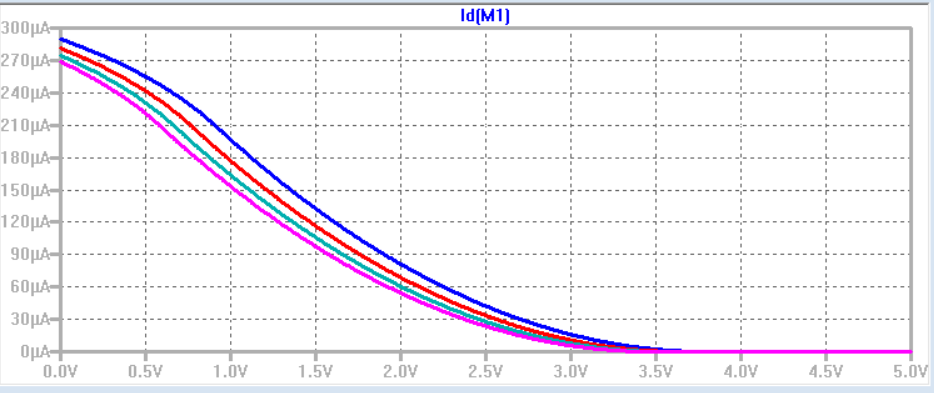
ID v. VGS (0 < VGS < 5 V) with VDS = 5 V for VSB varying from 0 to 3 V in 1 V steps.
NMOS:
LTSPICE:
Experimental Result:
using a sampling resistor of 1k-ohms. Varying VSB.
In
order to find the experimental result below, the VSB was varyed in
combination with the vds and vgs attached to a function generator
in order to get a Id Vs. Vds curve.
PMOS:
LTSPICE:
Experimental Result:
++++++++++++++
Experiment 2
++++++++++++++
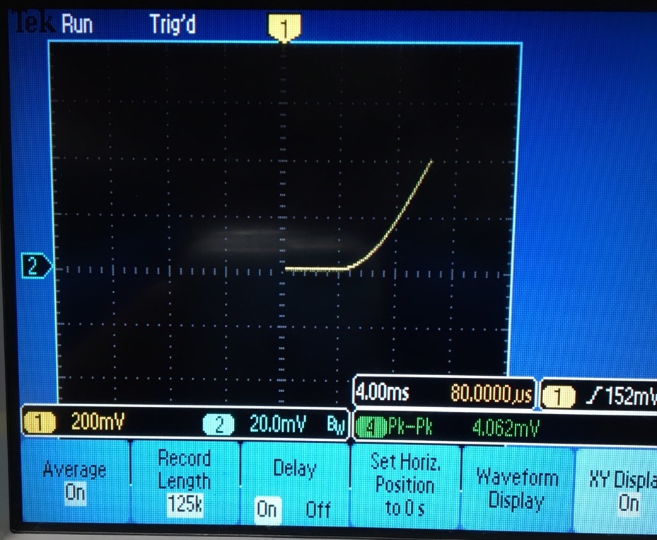
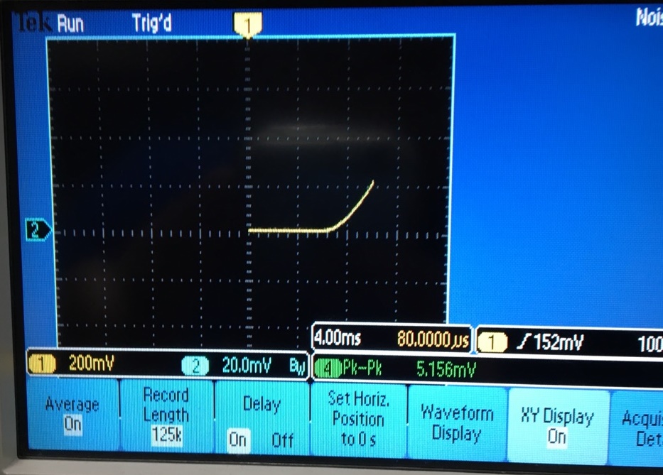
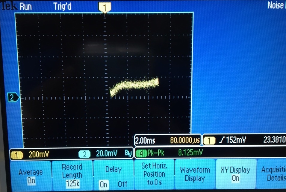
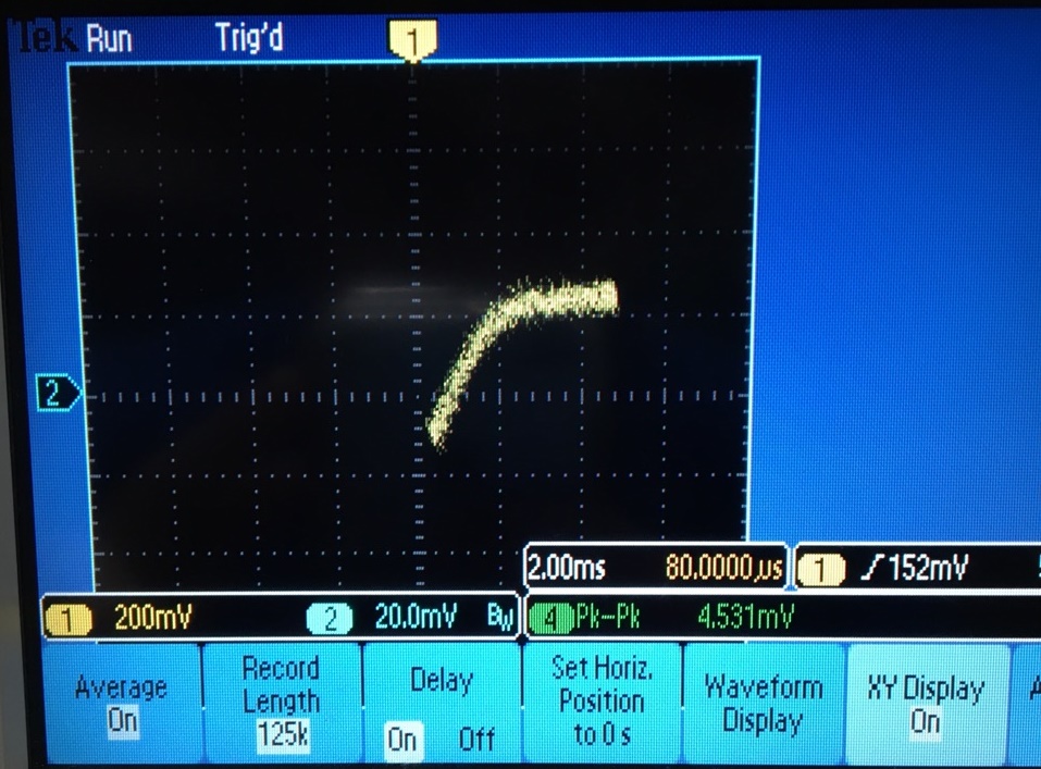
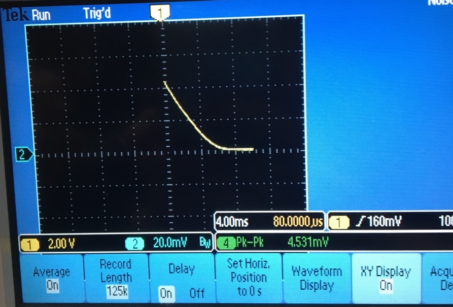
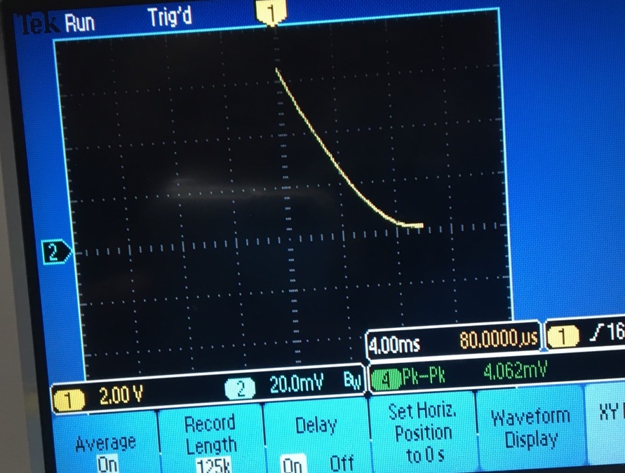
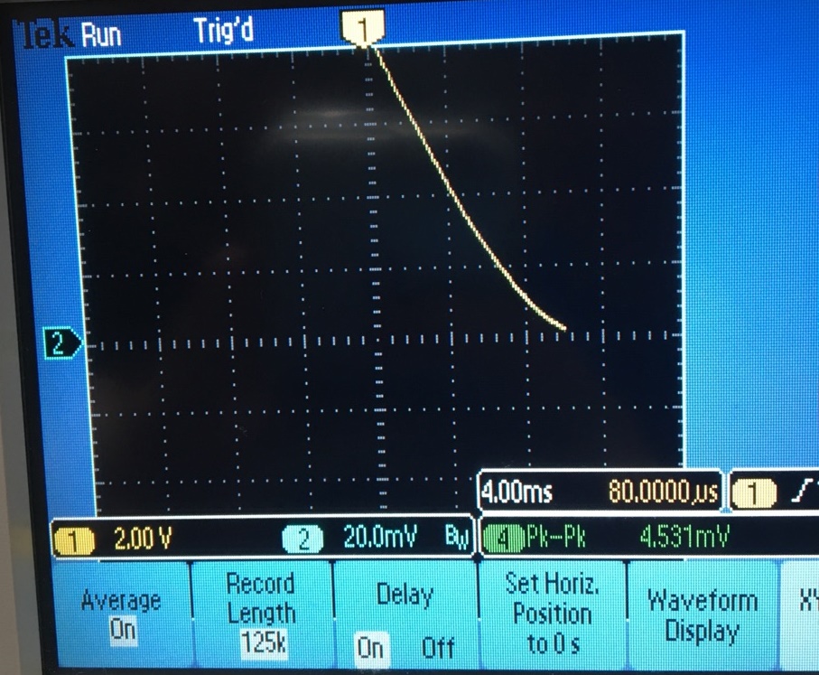
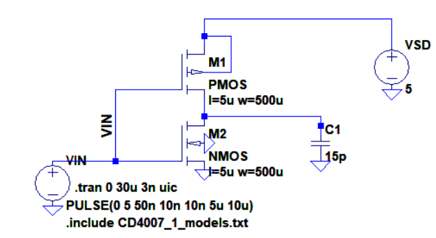
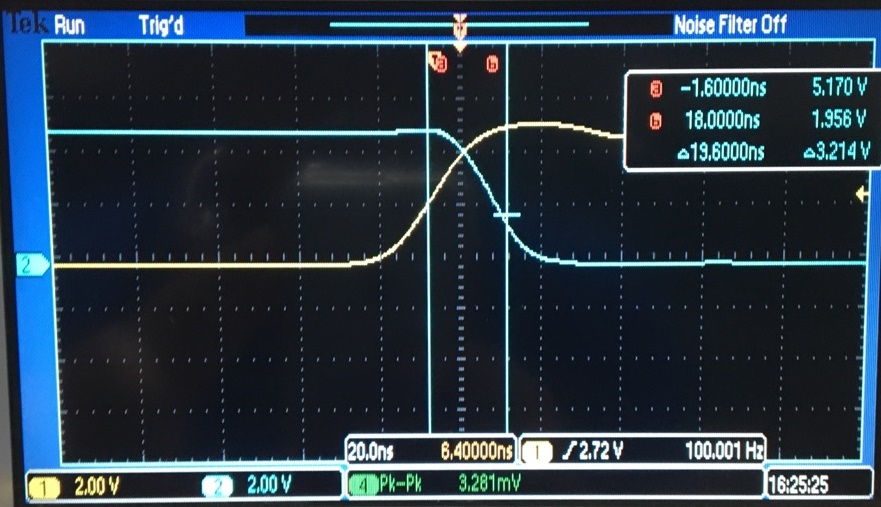
- Experimentally,
similar to what is seen on the datasheet (AC test circuits seen on page
3 of the datasheet), measure the delay of an inverter using these
devices (remember the loading of the scope probe is around 15 pF and
there is other stray capacitance, say another 10 pF).
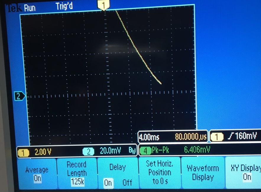
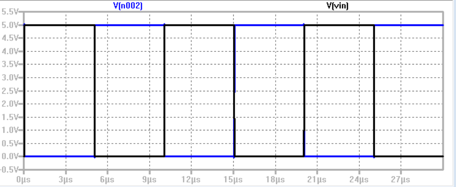
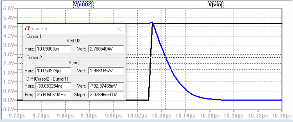
- Using
your model simulate the delay of the inverter and compare to measured
results. Adjust your SPICE model to get better matching between the
experimental data and the measured data.
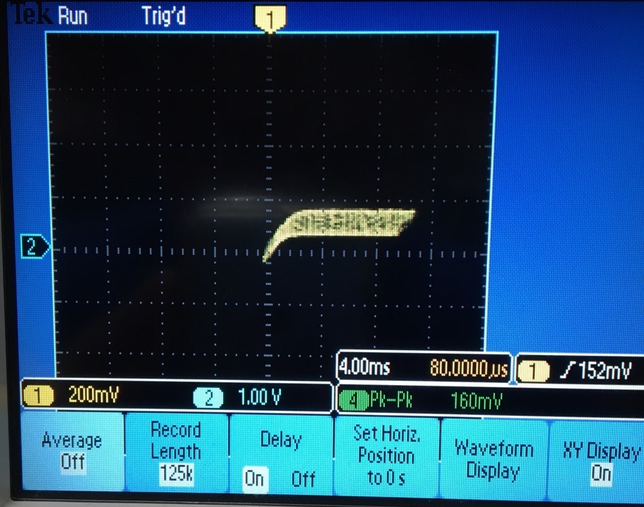
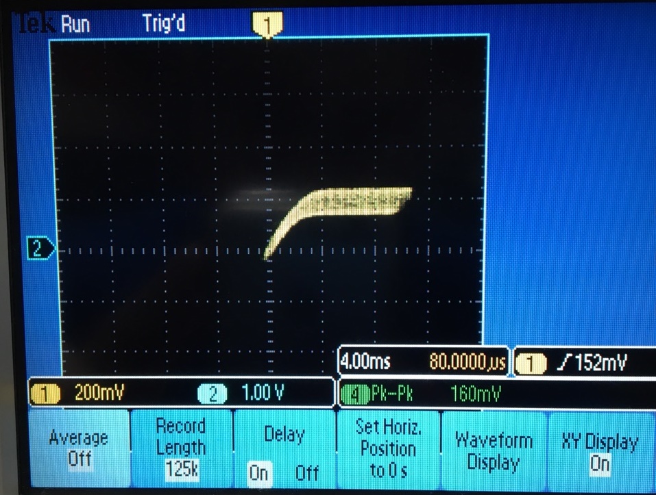
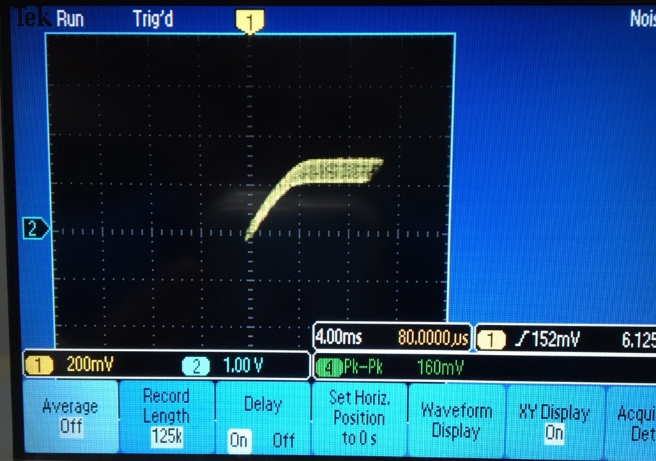
The rise and fall times closely match the datsheet specs.
++++++++++++++++++++++++++++++++++++++++++++++++++++++++++++++++++++++++++++++++
Lab Conclusion:
The
lab taught me how to test an NMOS and PMOS devices for its
characteristics. It taught me how to understand how a real world pmos
or nmos and how it can vary in terms of voltage sweeps in points of the
system; and what are good ways to figure out its thershold
voltage.
Return to EE 420L Labs