Lab 6 - ECE 420L Engineering Electronics II Lab
Authored
by Frank Sanchez,
sanchezf@unlv.nevada.edu
3/22/2017
++++++++++++++
Experiment 1
++++++++++++++
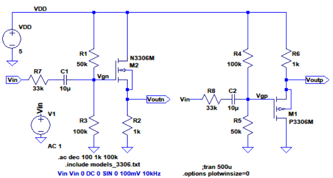
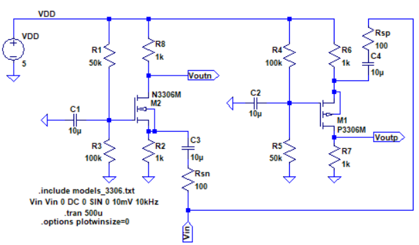
- Below are schematics for NMOS and PMOS source followers amplifiers (also known as common-drain amplifiers).
In your lab report discuss the operation of these circuits.
You
know that the circuit above can be measured from the source or output
terminal. The common-drain amplifier is used to output a voltage gain
of 1, with a current gain. To achieve current gain in the circuit, the
R2 resistor on the Vout pin creates a potential between the body(tied
to ground) and the source; an increase in in threshold voltage
consequently causes a current gain. The voltage divider on the gate is
there to bias the potential and determine the VGS. A capacitor is used
for AC coupling on the input voltage, in order to keep the bias in tact
at the gate.
Hand
calculate, and then verify your hand calculations with experimentation
and simulations, the gains and the input and output
resistances ensuring that your test signals are at a high enough
frequency that the caps have negligible impedance but not so high that
the gain is dropping off.
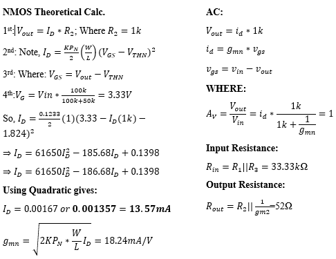
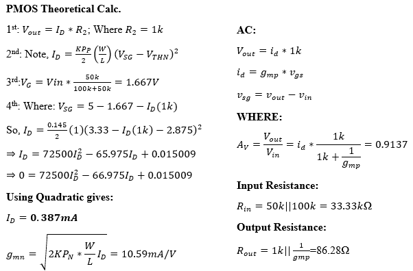
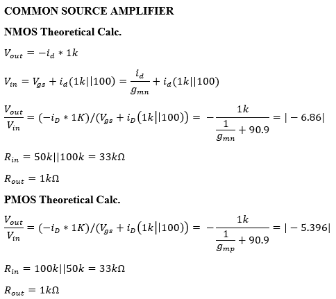
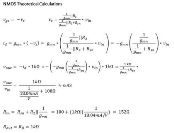
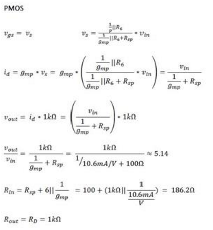
Theoretical Calculations
Simulate the operation of these amplifiers.
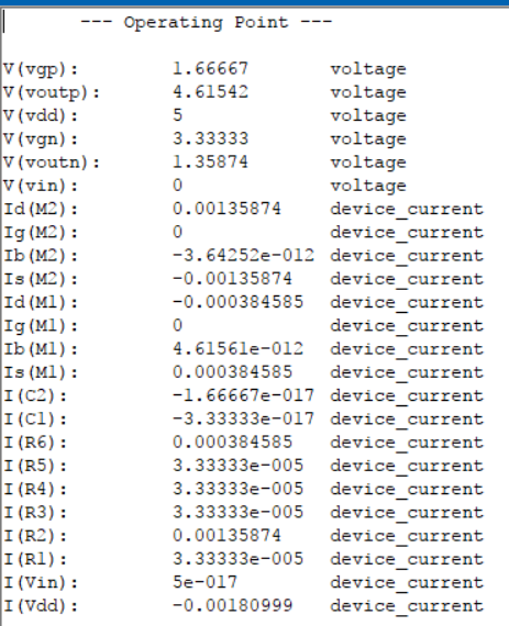
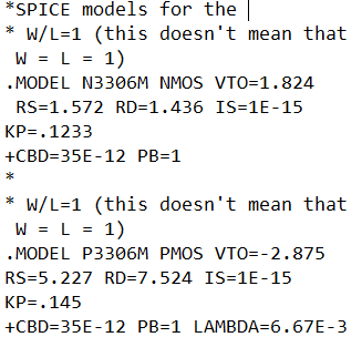
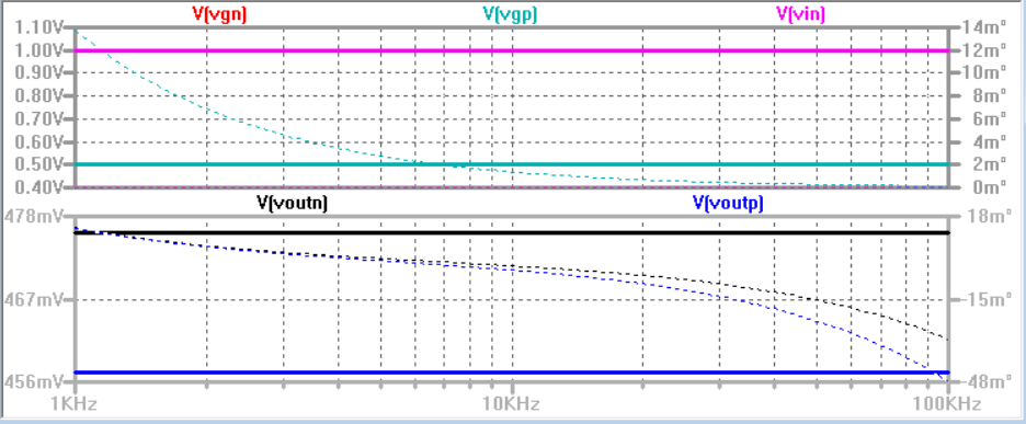
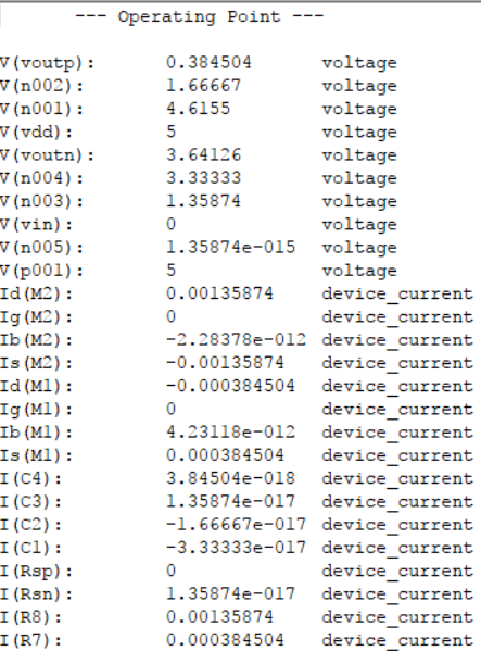
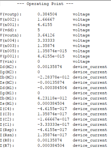
The images to the Below, displays the simulated DC voltages for the circuit; along with the transistor paramters used for the lab.
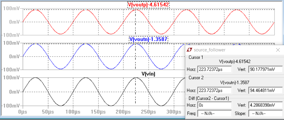
The
Transient Simulation for the circuit above shoes the NMOS GAIN of about
0.946 and a PMOS GAIN of about 0.9017 for a 100mV input voltage.
In your lab report discuss, in your own words, how to measure the input resistance.
In
order to measure the input resistance in LT spice and the lab
experiment , one must add an equivalent resistor calculated for both
NMOS and PMOS, respectively, and place it in series to the input
resistance. This in hand, forms a voltage divider that would give you
1/2 the input voltage; and 1/2 the output voltage. This is done for
both the NMOS and PMOS transistors.
Again, in your lab report discuss how to measure the output resistance.
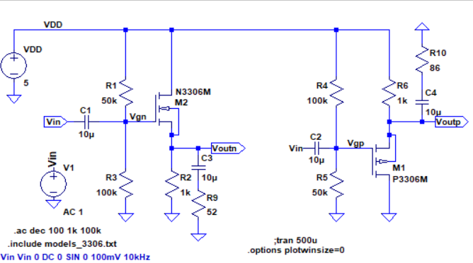
Similarly
to the input resistance, we can use the theoretical value calculated
for both the PMOS and NMOS transistors. Which are 86.28-ohms (PMOS) and
52-ohms(NMOS). A coupling capacitor in series with the calculated
resistor can be place in parallel to the respective transistors'
source. The output voltage is now connected to a voltage divider that
will result as 1/2 the output voltage.
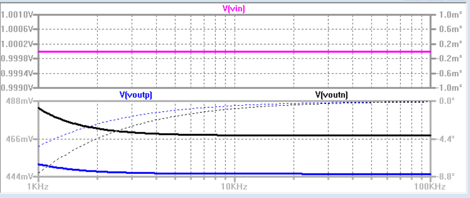
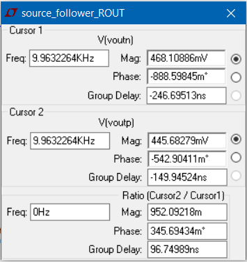
Simulation Below shows the measurement of the output resistance and the resulting waveforms displayed.
If
you build this circuit using electrolitic capacitors, assuming the
input AC signal swings around ground, put the "+" terminal of the cap
on the gate of the MOSFET. Please indicate, in your lab report, that you
understand why the capacitor is connected this way.
By
implementing an electrolitic capacitor for the design above, you must
understand that they are polarity sensitive. The electrolitic capacitor
uses a chemical reaction between the anode and the cathode to form an
insulating layer. If the capacitor is to become reversed-biased, the
capacitor would
inevitable create a short between the terminals. The result of any
significant voltage going across the capacitor can overheat and explode
the capacitor. Hence, its best to put the greater postive voltage in te
positive terminal of an electrolitic capacitor.
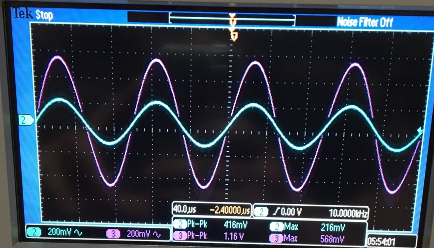
Experimental Results
All experiments used 10kHz input frequency
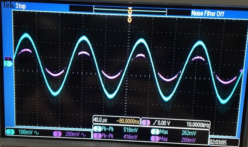
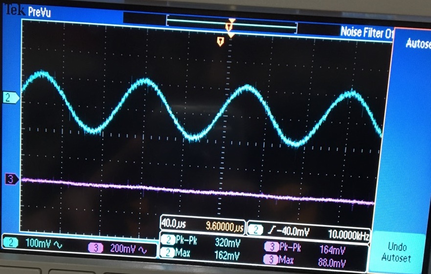
GAIN: NMOS(LEFT): Av=0.913. PMOS(RIGHT): Av=0.8.
Rin: NMOS(LEFT); PMOS(RIGHT).
The NMOS output is approximately one-half the input displayed. The same results for the PMOS.
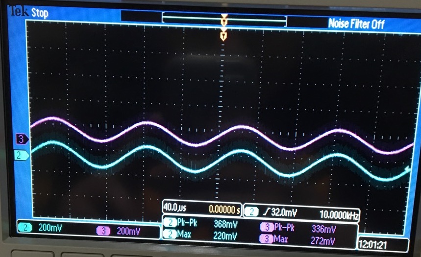
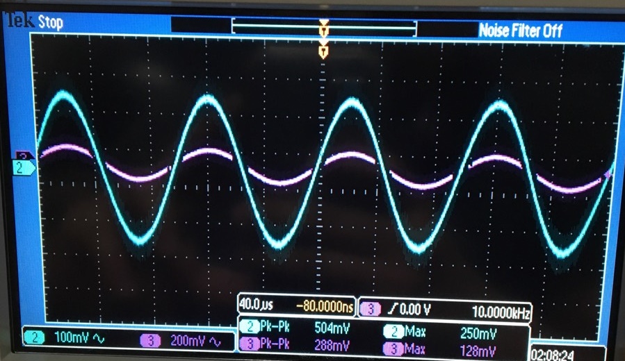
Rout: NMOS(LEFT); PMOS(RIGHT).
EXPERIMENT 1 TABLE
| NMOS | HAND | Simulation | Experimental | PMOS | HAND | Simulation | Experimental |
| GAIN | 0.948V/V | 0.946V/V | 0.913V/V | GAIN | 0.9137V/V | 0.9017V/V | 0.8V/V |
| RIN(OHM) | 33k | 33k | 33k | RIN(OHM) | 33K | 33K | 33K |
| ROUT(OHM) | 52 | 52 | 52 | ROUT(OHM) | 86 | 86 | 86 |
++++++++++++++
Experiment 2
++++++++++++++
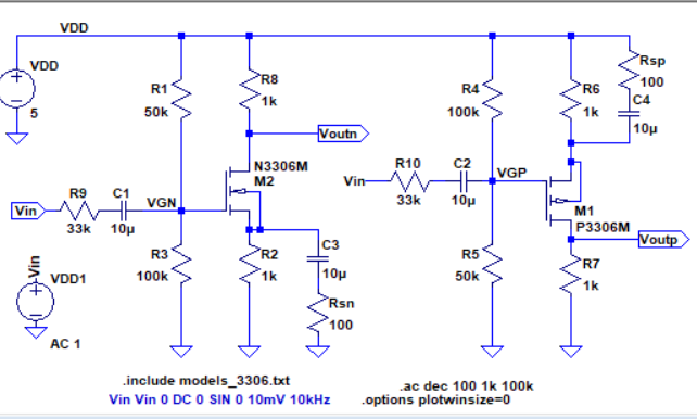
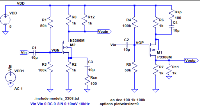
Common
Source Amplifiers are used for voltage amplifications. The CS amplifier
has the input at the gate and the output at the drain. The voltage
divider at the gate and the resistors in the drain and source provide
biasing and set saturation for the transistor. The capacitor is used
for AC coupling. CS is used for large gain.
Theoretical Results
Simulate the operation of these amplifiers.
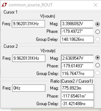
The images to the Below, displays the simulated DC voltages for the circuit; along with the transistor paramters used for the lab.
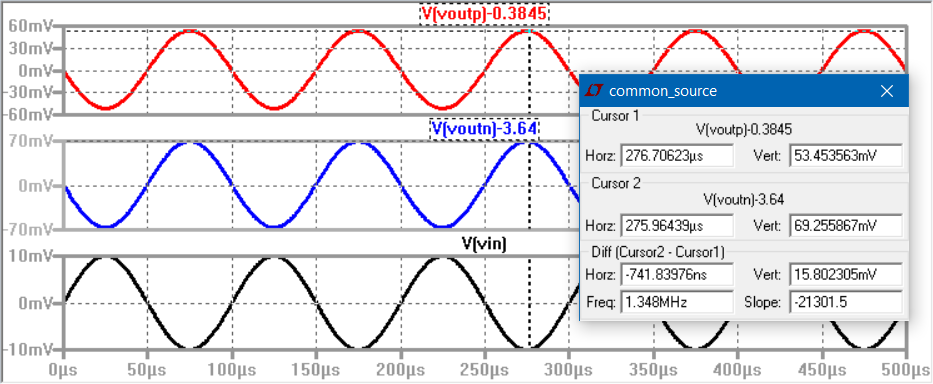
Gain for both CS amplifiers using 10mV input gave : NMOS Gain: Av=6.925; PMOS Gain : Av=5.34
In your lab report discuss, in your own words, how to measure the input resistance.
In
order to measure the input resistance in LT spice and the lab
experiment , one must add an equivalent resistor calculated for both
NMOS and PMOS, respectively, and place it in series to the input
resistance. This in hand, forms a voltage divider that would give you
1/2 the input voltage; and 1/2 the output voltage. This is done for
both the NMOS and PMOS transistors.
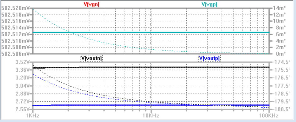
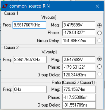
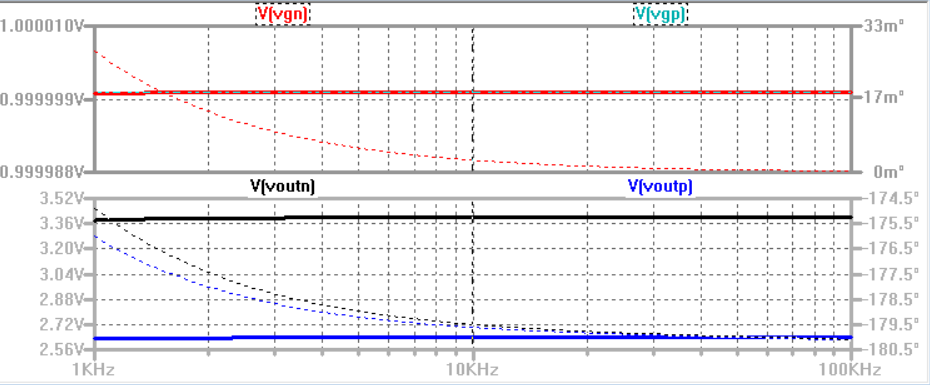
Shown below is the VGN and VGP output voltage of about 500mV. Which is half of the simmed input of 1V.
ROUT:
The
NMOS and PMOS waveform shows a gain that is one-half the initial gain
prior to addin the 1k-ohm resistor on the vout terminal.
Which was
Notice
that the NMOS and PMOS Gain was equivalent to 6.86V/V and 5.39V/V
respectively. Hence proving theoretical that the placed 1k resistor is
halving the output gain potential.
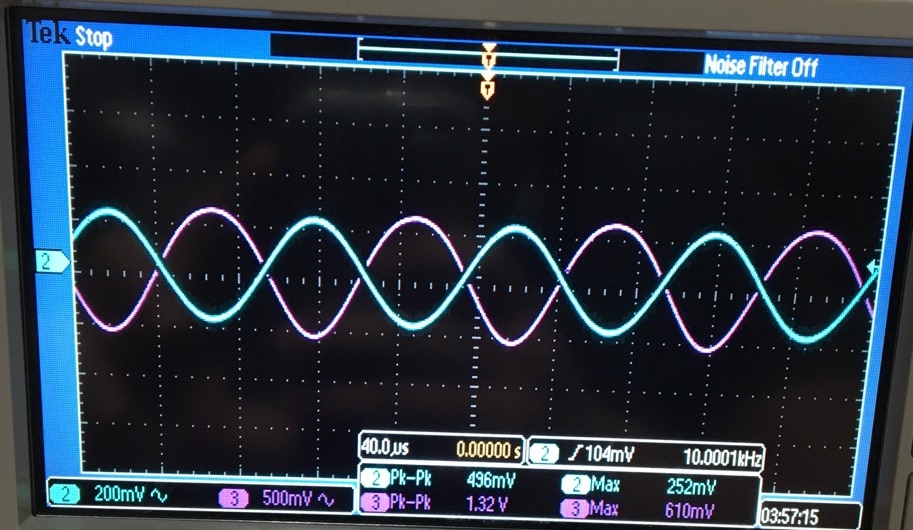
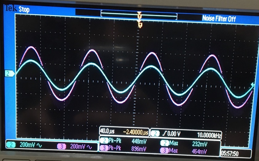
Experimental Results
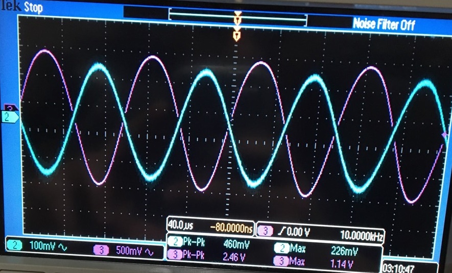
GAIN: NMOS: Av=5.3; PMOS: Av=2.8
The
NMOS input displays a 460mV pk-k and the output on channel 3 displays
2.46V pk-pk, resulting in a gain of 5.3. For the PMOS simulation on the
the input voltage on channel 2 was 486mV while the output voltage on
channel 3 was about 1.36V; giving a calculated gain of around 2.8. The
PMOS result didn't meet its theoretical expectactions. The PMOS circuit
was retested multiple times in order to meet specifications, but the
gain of 2.8 was the best tried attempt at the theoretical.
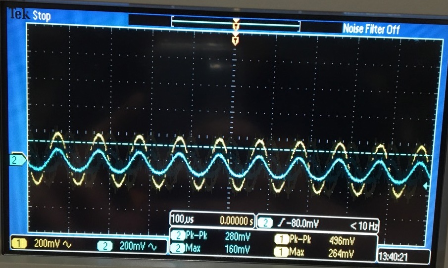
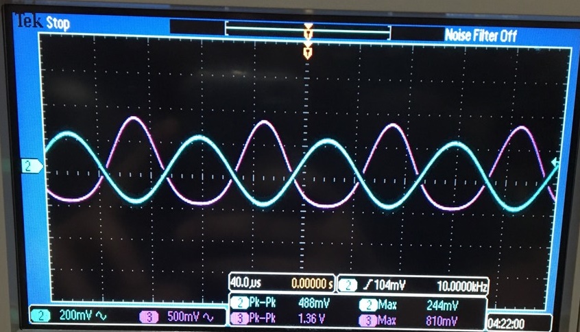
Rin:
RIN
was measured experimentally the same as in the LT spice simulation. The
NMOS(LEFT) result below displays the output at around 200mV which is
half the potential the input voltage is supplying. meaning a gain of
about half when comparing it to the inital voltage gain with the added
resistor value.
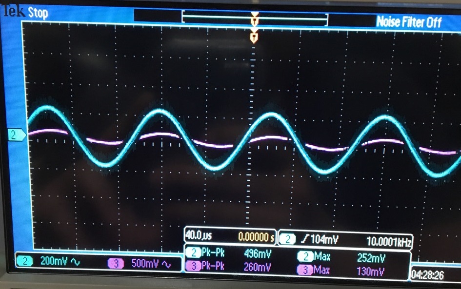
Same goes for the PMOS(right), The potential after the included resistor value was about 260mV on channel 3.
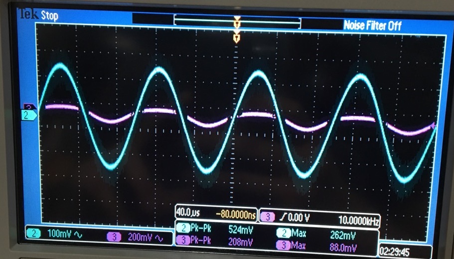
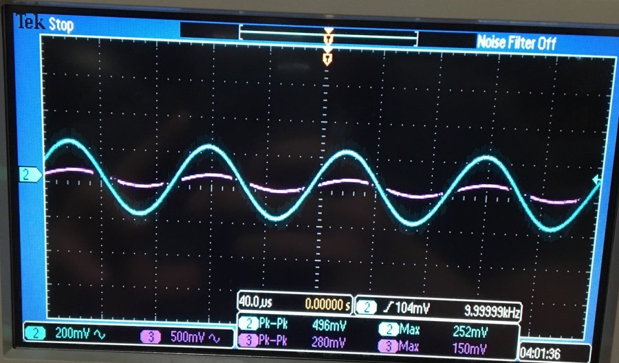
Rout:
The
NMOS(LEFT) waveform for ROUT is displayed below. The output gain of
about 1.32V, which is close to half the initial gain acquired for the
NMOS circuit without the added resistor. The PMOS(RIGHT) waveorm for
ROUT is displayed below. The output gain of about 700mV, which is close
to half the initial gain acquired for the PMOS circuit without the
added resistor. The voltage divider functioned as expected and handed
me a pretty close estimate to the theoretical calculations.
EXPERIMENT 2 TABLE
| NMOS | HAND | Simulation | Experimental | PMOS | HAND | Simulation | Experimental |
| GAIN | -6.86V/V | 6.8V/V | 5.3V/V | GAIN | -5.396V/V | 5.39V/V | 2.8V/V |
| RIN(OHM) | 33k | 33k | 33k | RIN(OHM) | 33K | 33K | 33K |
| ROUT(OHM) | 1k | 1k | 1k | ROUT(OHM) | 1k
| 1k | 1k |
++++++++++++++
Experiment 3
++++++++++++++
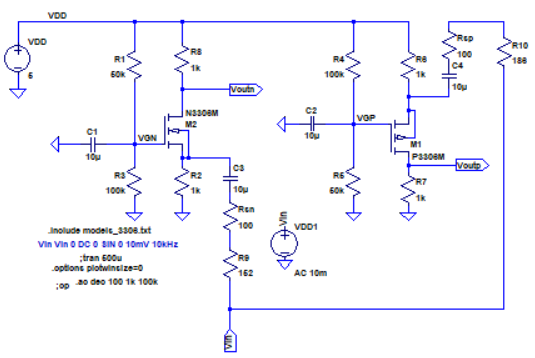
The
common gate has the input on the source and the output on the drain.
The CG amplifier has the low input impedance and high ouput impedance.
The result gives high-voltage gain, with low current and power gain.
This circuit is dc biased th same way as the source follower. The
source resistances are inversely proportional to the gain and cause the
gain to increase when the are decreased.
Theoretical Results
Simulate the operation of these amplifiers.
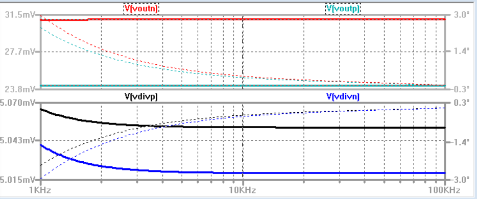
The current in each device is the same as the gate voltages. The same process was used to find the RIN and ROUT for the design.
The
gain for both the CG amplifiers is similar to the thoretical results
calculated. The Gain for the NMOS was about 6.22. The PMOS gain was
around 4.76. This in hand, using a 10 mV input sorurce.
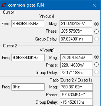
RIN SIMULATION:
Note
that the voltage output is approximately one-half the output gain from
the initial voltage gain shown above. This verifies the input
resistance is accurate to the theoretical results calculated by hand.
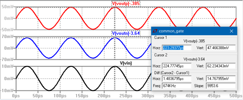
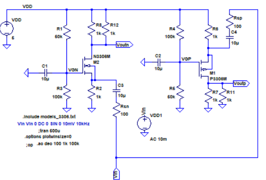
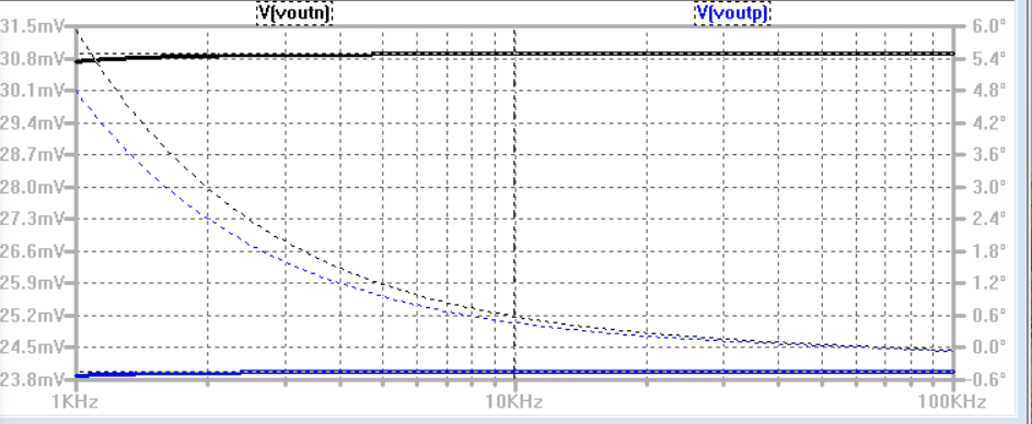
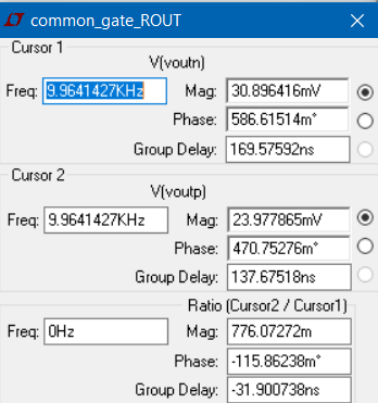
ROUT SIMULATION:
The
NMOS in the waveform below displays a 30.8mV output on a 10mV. In
comparison, the initial output gain without the voltage divider gave me
a value of 62.2V. Which in hand relates to a half output voltage when
applying the resistor to the desgn. The same is shown for the PMOS
design. Once again, the simulation verifies the theoretical output
resistance.
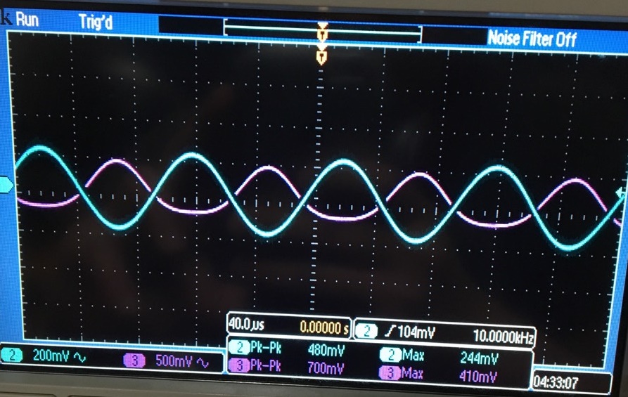
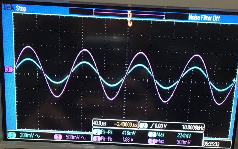
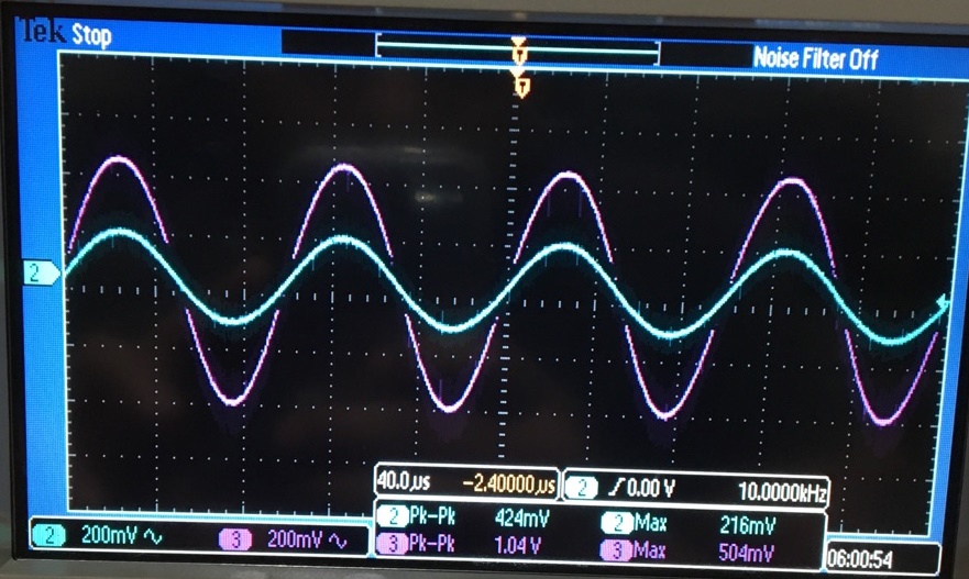
Experimental Results:
GAIN: NMOS(lLEFT): Av= 4.7 ; PMOS(RIGHT): Av= 2.6
The
GAIN displayed to be 1.86/.416, or around 4.7. This result was a little
off, but thegain was there.Same went about the PMOS gain. As the output
voltage shoed a 1.22V result with a gain of 2.6.
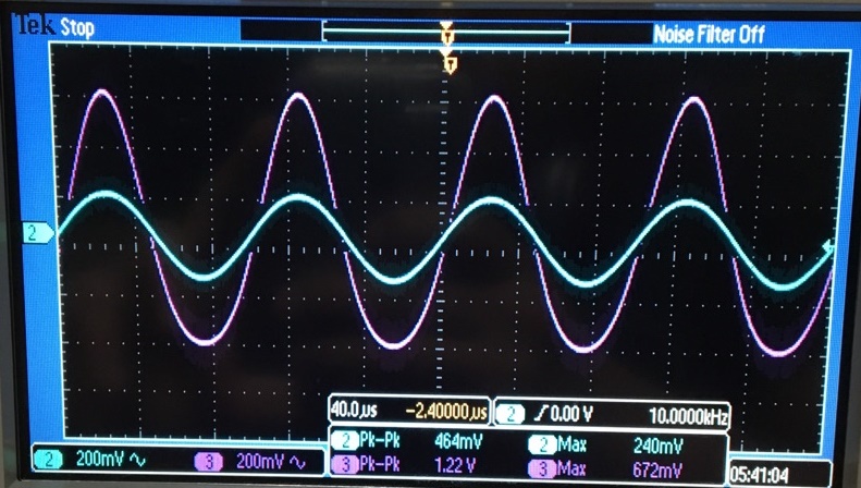
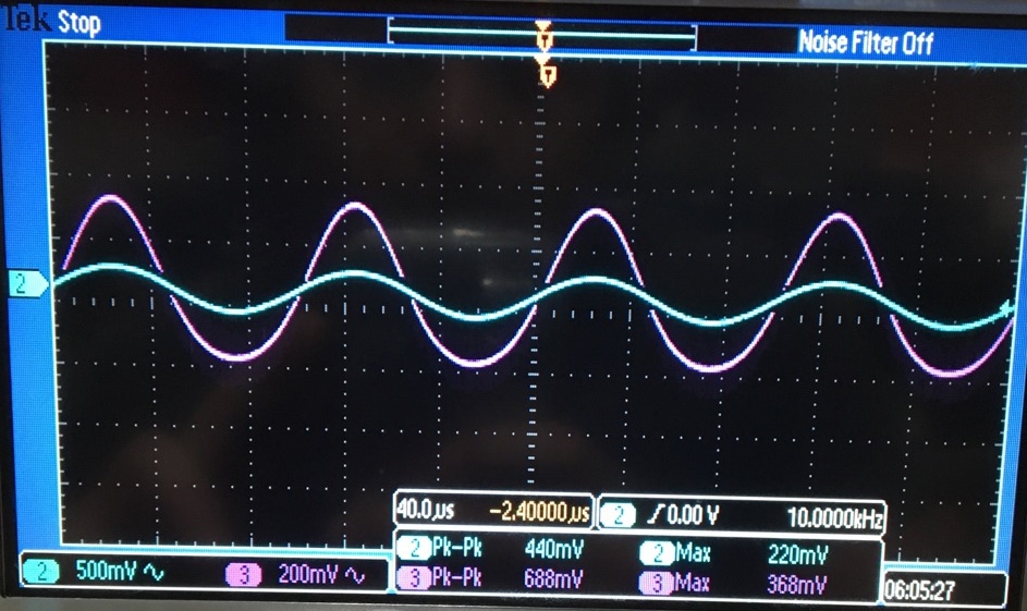
RIN: NMOS(LEFT); PMOS(RIGHT)
RIN
is measured the same was as done before. The NMOS wavefor displays the
one-half the initial gain after adding the 152-ohm resistor to the
input as the simulation schematic. This in hand confirms the input
resistance calculation is accurate to the theoretical result. The PMOS
output wavefor shows a similar result. In hand very close to half the
output gain.
ROUT: NMOS(LEFT) ;; PMOS(RIGHT)
The
NMOS output waveform displays aproximately one-half of the initial
output gain simulated above. This came about with the addition of the
1k-ohm resistor on the design. The PMOS showed similar results.
EXPERIMENT 3 TABLE
| NMOS | HAND | Simulation | Experimental | PMOS | HAND | Simulation | Experimental |
| GAIN | -6.43V/V | .6.21V/V | 4.7V/V | GAIN | 5.14V/V | 4.76V/V | 2.7V/V |
| RIN(OHM) | 152 | 152 | 152 | RIN(OHM) | 186 | 186 | 186 |
| ROUT(OHM) | 1k | 1k | 1k | ROUT(OHM) | 1k
| 1k | 1k |
++++++++++++++
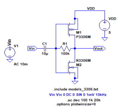
Experiment 4
++++++++++++++
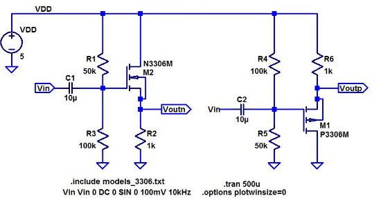
PUSH-PULL AMPLIFIER
Discuss the operation of this amplifier in your lab report including both DC and AC operation. Hand calculate the
gain of this amplifier. Do you expect this amplifier to be good at
sourcing/sinking current? Why or why not? What happens to the gain if
the 100k resistor is replaced with a 510k resistor? Why?
The
transistors are used in harmony in order to output a high efficiency
and high output power. The push pull amplifier is designed to have an
output that can drive current through the load by either load or pull.
at a high voltage gain. The input and output are tied by the 100k-ohm
resistor allowing the cirucit to be self biased with no DC curren
in transistors. If an input current is negative, causes the M1
transistor to increase and turn on while increasing the the M2 untile
it shuts off. The opposed can be said with a positive current.This in hand is called a class AB amplifier.
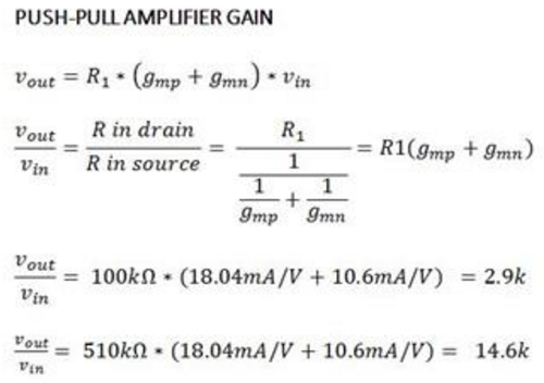
The amplifier gain is related to the resister on the design, as shown below.
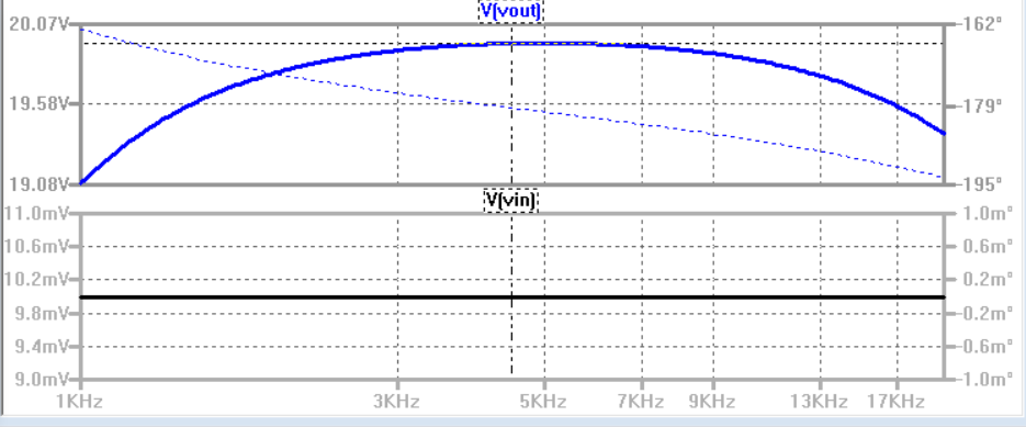
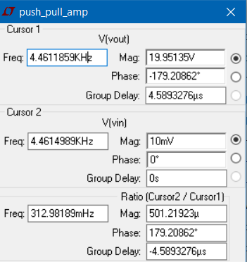
Simulation Results:
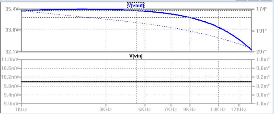
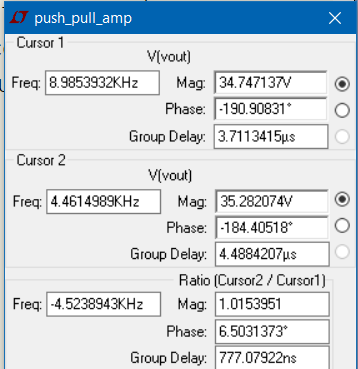
Using a 10mV input, I got around 20V output. Which is around 2k V/V.
PART 2: 510K
At 510k ohms, the gain wil increas which can be seen though the gain formula above.
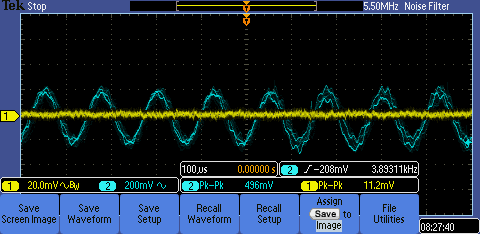
Experimental Results:
100k
510kExperiment 4 Table
| PUSH-PULL | HAND | SIMULATION | EXPERIMENTAL |
| GAIN | 14.6K | 3.45K | |
| GAIN | 2.9KV/V | 2KV/V | 1.6k |
+++++++++++++++++++++++++++++++++++++++++++++++++++++++++++++++++++++++++++++++
Lab Conclusion:
The
lab gave the stundent to understand single stage transistor amplifiers.
The lab gave us an in depth look and on how common drain (CD), common
source (CS), common gate (CG), and push-pull amplifiers. The
simulations and experiments conducted in the lab gave me the insight
on how these practical applications can be used in specific ways;
and on how to understand the differences between real-world
application, and theoretical application.
Return to EE 420L Labs