Lab 3 - ECE 420L Engineering Electronics II Lab
Authored
by Frank Sanchez,
sanchezf@unlv.nevada.edu
2/15/2017
For the following questions and experiments assume VCC+ = +5V and VCC- = 0V.
- Knowing
the non-inverting input, Vp, is at the same potential as the inverting
input, Vm, (called the common-mode voltage, VCM) what are the maximum
and minimum allowable common-mode voltages?
- Support your answer with an entry from the electrical characteristics table in the datasheet.
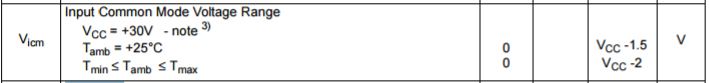
The maximum allowable common-mode voltage is Vcc-1.5V. While the minimum voltage is 0V at +25 C.
This is indicated in the datasheet provided. The image below are values
for the LM324 datasheet. While the Vcc is rated for a maximum of 30V. So our range is 0V to 28.5V.
C.
This is indicated in the datasheet provided. The image below are values
for the LM324 datasheet. While the Vcc is rated for a maximum of 30V. So our range is 0V to 28.5V.

- What is a good estimate for the op-amp's open-loop gain?
- Support your answer with a plot from the datasheet and an entry from the electrical characteristics table.
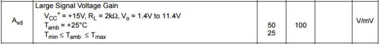
The table below indcates the gain of 100V/mV.
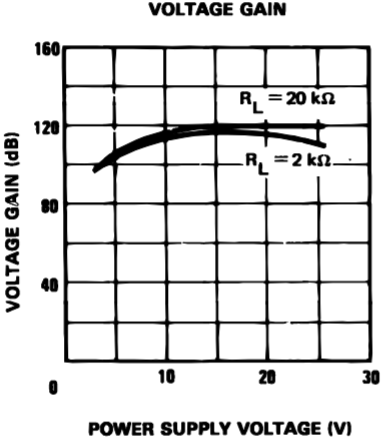
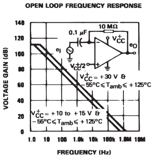
The
voltage gain graph below indicates the different gains per varying
power supply voltage.The open-loop frequency response graph below
indicates a gain of 100dB.
- What is a good estimate for the offset voltage?
- For worst case design what value would you use?
According to the datasheet, a typical volate is 2mV. With a high temperature, are highest value would end up being 9mV offset. 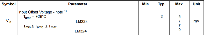
++++++++++++++++++++++++++++++++++++++++++++++++++++++++++++++++++++++++++++++++++++++++++++++++++++++++++++++
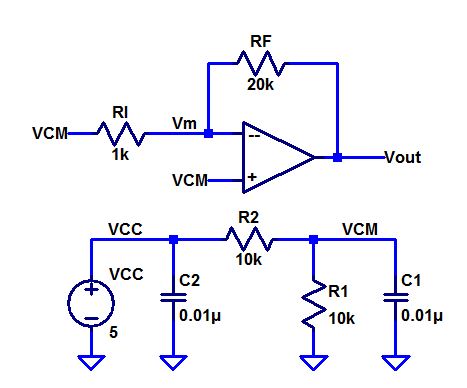
Build,
and test, the following circuit. Note that a precise value for the 5k
resistors isn't important. You can use 4.7k or a 5.1k resistors.
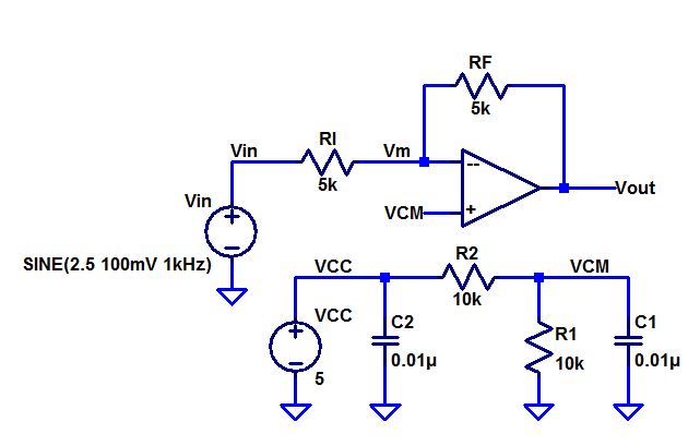
- What is the common-mode voltage, VCM? Does VCM change? Why or why not?
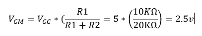 The
circuit above contains a voltage divider; that in hand should make a
VCM equal to 2.5V. As shown below, the experimental result was close to
the theoretical.
The
circuit above contains a voltage divider; that in hand should make a
VCM equal to 2.5V. As shown below, the experimental result was close to
the theoretical.
 ]
]- What is the ideal closed-loop gain?
The circuit used has an inverting op-amp topology. The ideal closed-loop gain is:
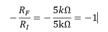 which in hand is 180
 out of phase.
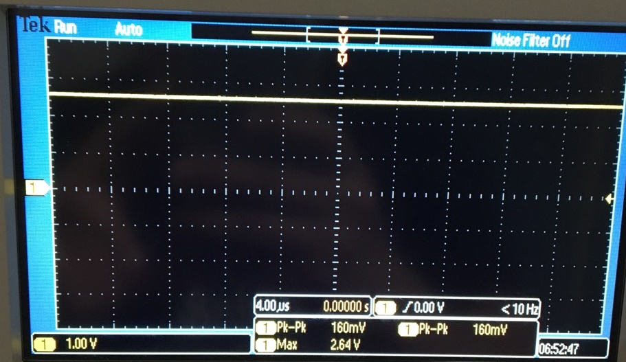
- What is the output swing and what is it centered around?
- What happens if the input isn't centered around around VCM, that is, 2.5 V?
- Provide a detailed discussion illustrating that you understand what is going on.
The output swing is the voltage the op-amp provides; as shown below, you can see that the output is 180degrees out of phase.
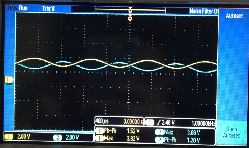
If
the input isn't centered arond VCM, the output signal changes. We
wouldnt get the full swing of 2.5V/amplitude. The output swing cant
exceed the values of [ 5VCC+ or 0VCC-]
- What is the maximum allowable input signal amplitude? Why?
Anything larger than the input signal of 2.5V will get clipped; for it would exceed the value of the supplied voltage.- What is the maximum allowable input signal if the magnitude of the gain is increased to 10? Why?
250mV
would be the maximum allowable input signal, for it is determined by
the basis of the output voltage being centered at 2.5v. in rescpect to
the power supplied.

- What is the point of the 0.01 uF capacitors from VCC and VCM to ground?
- Are these values critical or could 0.1 uF, 1,000 pF, 1 uF, etc. capacitors be used?
The capacitors are mean to act as coupling capacitors, for they prevent noise.
The
values of the capacitors isn't critical; for they are only used for
decoupling.The capacitor acts as an open for DC, and a short for AC
signal.- The data sheet shows that this op-amp has an input bias current that flows out of the op-amp's inputs of typically 20 nA.
- This current flows out of both the non-inverting and inverting inputs through the resistors connected to these inputs.
- Show how the operation of the circuit can be effected if, for example, R1 and R2, are much larger. Explain what is going on.
If
the two resistors are much larger, the input bias current would make a
difference. Say a 1 MEG-ohm resistors in parallel with 20nA flowing
through; we would get a voltage drop of about .01V , which in hand is
added to the VCM of 2.5v. Meaning the output would clip for it woult
exceed the VCC limit of 0-5v. - What is the input offset current? What does this term describe
The input offset current is the difference between the input bias current of the op-amp terminals.
++++++++++++++++++++++++++++++++++++++++++++++++++++++++++++++++++++++++++++++++++++++++++++++++++++++++++++++
Explain how the following circuit can be used to measure the op-amp's offset voltage.
- Note that if the output voltage is precisely the same as VCM then the op-amp has no offset voltage (this is very possible).
- To measure small offset voltages increase the gain by increasing RF to 100k or larger. Explain what is going on.
Well
if the output voltage is the same as VCM, assuming an ideal op-amp. you
can measure the offset of the circuit. Consider its an inverting of
amp, you note 20k/1k= 20V/V gain. When measuring the offset , you
divide by 20.
When increasing the RF to 100k, you'd get a 100V/V; for it can help us see a very small offset.
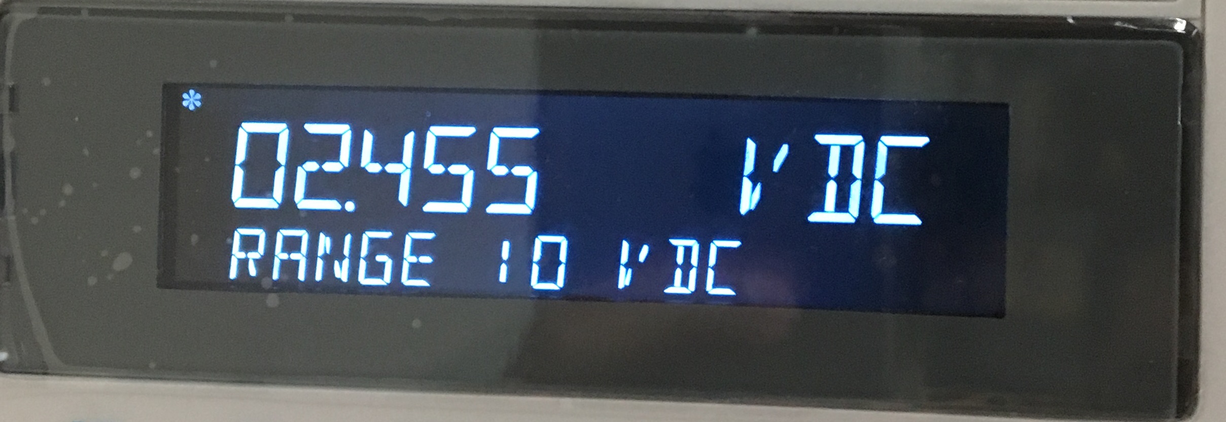
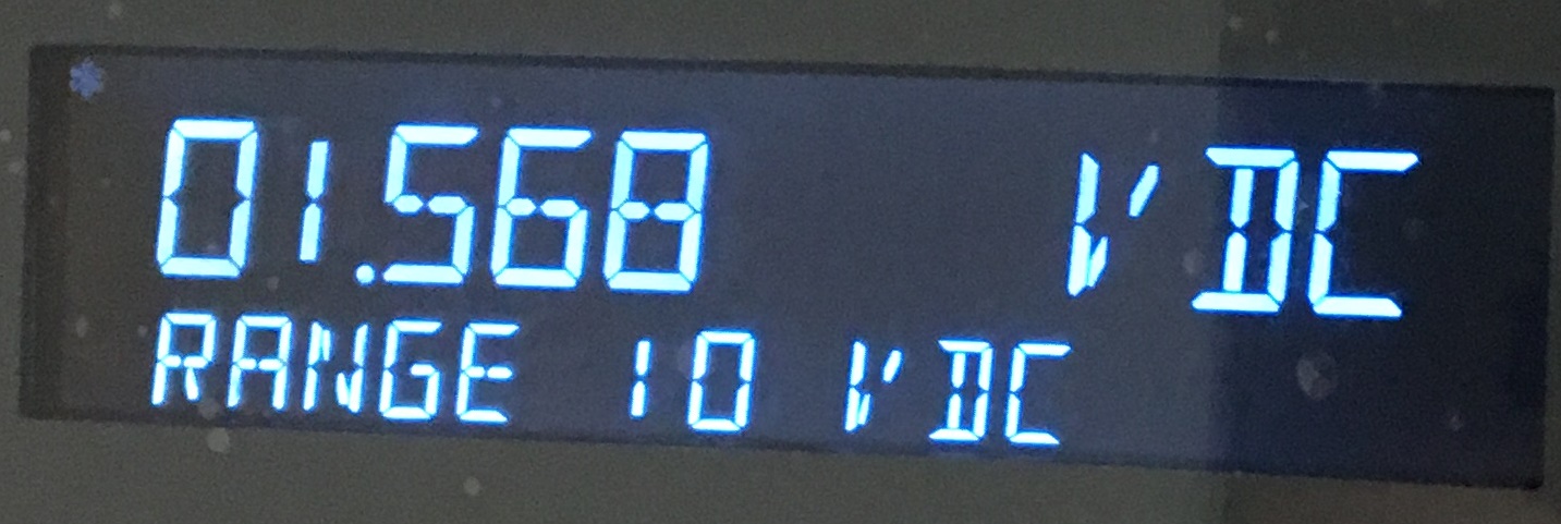
- Measure the offset voltage of 4 different op-amps and compare them.
Each
offset was different when using different op amps; showing the
importance of testing a chip beforhand if it can possiblly be a problem.
While the LCM is 0.2438V
Outputs are:
USED: LM324
lm393
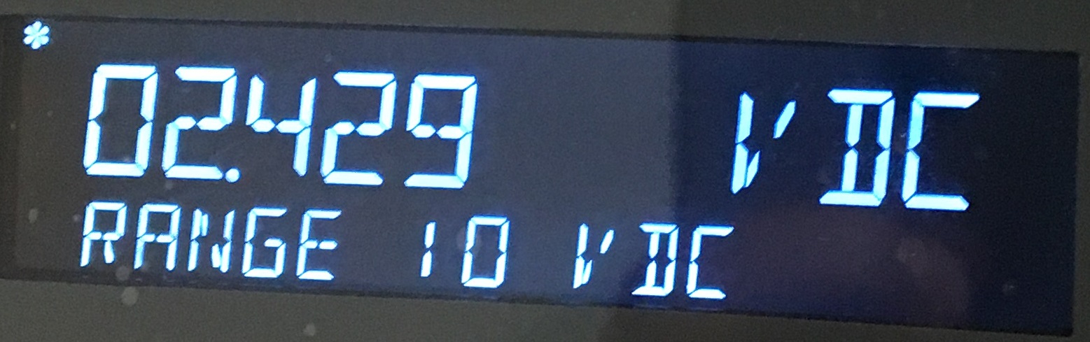
lf351
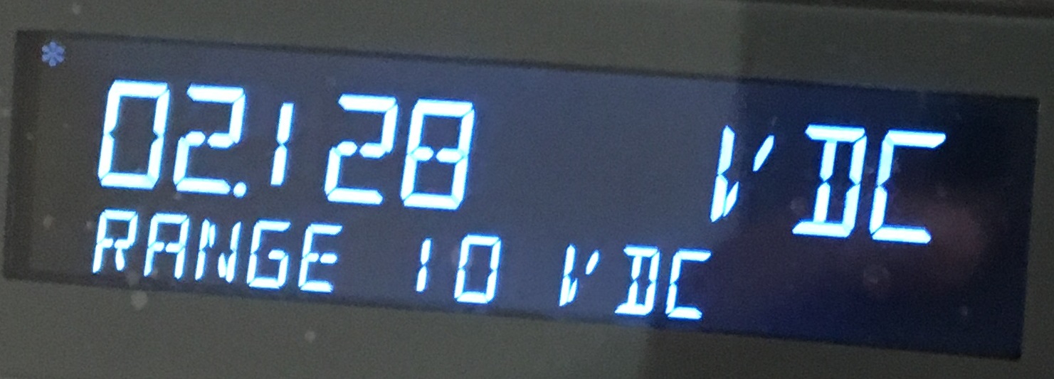
tl08
++++++++++++++++++++++++++++++++++++++++++++++++++++++++++++++++++++++++++++++++
Conclusion:
This
lab gives us some insight on how ap-amps work, and how a small or large
voltage peak inputs can influence the output signal of an op-amp;
non-inverting or inverting. This lab also showed us how to look up
information on datasheets for op-amps.
Return to EE 420L Labs