Lab8 - EE 420L
Authored
by Allan Pineda
pineda3@unlv.nevada.edu
February 15, 2017
Lab Description: Characterization of the CD4007 CMOS transistor array
Pre-lab work:
- Review the datasheet for the CD4007.pdf CMOS transistor array.
- Ensure
to understand how the bodies of the NMOS are tied to pin 7 (VSS,
generally the lowest potential in the circuit, say ground)
- Bodies of the PMOS are tied to pin 14 (VDD, generally the highest potential in the circuit, say + 5V).
Experiment 1
In
this laboratory experiment, CD4007 transistor will be characterized and
generate a spice level=1 models. The maximum level power will be use to
characterize the transistor is +5V.
The first device to be
characterize is the NMOS. The goal is to generate ID vs VGS
plots from 0V to 3V with VDS of 3V, ID vs VDS plot
from 0V to 5V with VGS varying from 1V to 5V in 1V steps, and ID vs VGS
from 0V to 5V with VDS = 5V from VSB varying from 0 to 3V in 1 V
steps.See Figure below.
NMOS:
ID vs VGS plots from 0V to 3V with VDS of 3V:


Waveform Varying VGS from 0V to 3V
Schematic Varying VGS from 0V to
3V
ID vs VDS plot from 0V to 5V with VGS varying from 1V to 5V in 1V steps:


NMOS Schematic
VGS = 1


Waveform VGS = 2
Waveform VGS =
3


Waveform
VGS = 4
Waveform VGS = 5
ID vs VGS from 0V to 5V with VDS = 5V from VSB varying from 0 to 3V in 1 V steps.See Figure below:


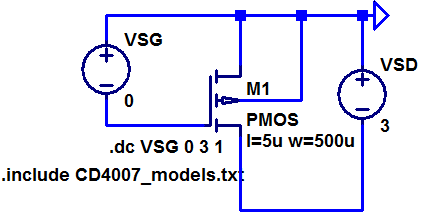
PMOS:
The second device to be
characterize is the PMOS. The goal is to generate ID vs VSG
plots from 0V to 3V with VSD of 3V, ID vs VSD plot
from 0V to 5V with VSG varying from 1V to 5V in 1V steps, and ID vs VSG
from 0V to 5V with VSD = 5V from VBS varying from 0 to 3V in 1 V
steps.See Figure below.
At this point of the experiment, a multi-meter was use to find all paramater of the PMOS device.
ID vs VSG plots from 0V to 3V with VSD of 3V:


ID vs VSD plot from 0V to 5V with VSG varying from 1V to 5V in 1V steps:


Schematic
Waveform Result
VARYING VSD


VARYING VSG


| ID vs VSD; Varying VSG=1 | ID vs VSD; Varying VSG=2 | IDvs, VSD Varying VSD=3 | IDvs, VSD Varying VSD=4 | IDvs, VSD Varying VSD=5 |
| VSD = 0; ID=0 | VSD = 0; ID=0 | VSD = 0; V= 0 ID=0 | VSD = 0; ID=0 | VSD = 0; ID=0 |
| VSD = 1; ID=1u | VSD = 1; ID=38.3u | VSD = 1; ID=72u | VSD = 1; ID=144u | VSD = 1; ID=290u |
| VSD = 1.7; ID=50u | VSD = 1.7; ID=192.6u | VSD = 1.7; ID=450u | VSD = 1.7; ID=906u | VSD = 1.7; ID=1760u |
| VSD = 1.9; ID=68u | VSD = 1.9; ID=251.6u | VSD = 1.9; ID=820u | VSD = 1.9; ID=1305u | VSD = 1.9; ID=2150u |
| VSD = 2.7; ID=82u | VSD = 2.7; ID=320.8u | VSD = 2.7; ID=1034u | VSD = 2.7; ID=1760u | VSD = 2.7; ID=3240u |
| VSD = 3.9; ID=95u | VSD = 3.9; ID=403.7u | VSD = 3.9; ID=1080u | VSD = 3.9; ID=2160u | VSD = 3.9; ID=5400u |
| VSD = 4.2; ID=105u | VSD = 4.2; ID=435.7u | VSD = 4.2; ID=1200u | VSD = 4.2; ID=3241u | VSD = 4.2; ID=6480u |
| VSD = 4.2; ID=138u | VSD = 5.0; ID=450u | VSD = 5.0; ID=1221u | VSD = 5.0; ID=3375u | VSD = 5.0; ID=6615u |
ID vs VSD from 0V to 5V with VSG = 5V from VBS varying from 0 to 3V in 1 V steps.See Figure below:


Above
shows how to find the KP, VTO and current flowing in the circuit. In
part of NMOS oscilloscope was used to generate ID vs VDS curve and
estimate the current with respect to VDS. For PMOS, a combination of multimeter and oscilloscope was
use to measure voltage and calculate to the current to get the KP, VTo
and other parameters of the device to be able to simualte the data.
Experiment 2
This
experiment focus on calculations using collected data from previous
experiment. Here, one can calculate the parameter using the data from
the experiment above.
Given:
L = 5um, W = 500um, Cox = 5pF

Experiment 3
In this part of experiment, simulation done by using the parameter data obtain above.

NMOS:

NMOS
Schematic
NMOS Waveform

NMOS Schematic sweeping both VGS and VDS
NMOS Waveform sweeping both VGS and VDS


NMOS Schematic sweeping both VGS and VSB
NMOS Waveform
sweeping both VGS and VSB
PMOS:

PMOS Schematic
PMOS Waveform

PMOS Schematic sweeping both VSG and
VSD
PMOS Waveform sweeping both VSG
and VSD


PMOS Schematic sweeping both VSG
and VBS
PMOS Waveform sweeping both
VSG and VBS
Experiment 4


From Data Sheet
Schematic
Schematic
Simulation

Push-Pull Waveform
Conclusion:
Thus
base on the data above, the estimated values use in experiment is
verifed through LTSpice since the values are not too far from each
otehr. This lab experiment is very useful for future reference. It
shows how to create a level=1 Spice list. Using oscilloscope is very
though compare to ammeter to measure current. Using voltmeter and
ammeter will expedite the work but it require a more mathematical
calcualtion.