Lab 3 - ECE 420L
VCC+ = 5
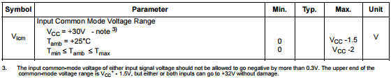
Knowing the non-inverting input, Vp, is at the same potential as the inverting input, Vm, (called the common-mode voltage, VCM) what are the maximum and minimum allowable common-mode voltages? Support your answer with an entry from the electrical characteristics table in the datasheet.
-0.3 < Vcm < 3.5 V
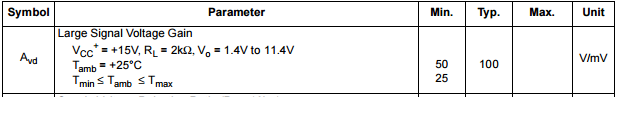
What is a good estimate for the op-amp's open-loop gain? Support your answer with a plot from the datasheet and an entry from the electrical characteristics table.
100mV /V or 100K
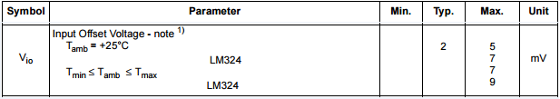
Typ 2 mV
Worst case 9 mV
What is the
common-mode voltage, VCM? Does VCM change? Why or why not?
VCM = 2.5 V It does not change because the
What is the ideal
closed-loop gain?
1 V
What is the output
swing and what is it centered around?
+/- 50 mV centered around 625 mV
What happens if the
input isn't centered around around VCM, that is, 2.5 V?
In this configuration the output and VCM will remain stable,
but Vm will maintain its current relationship to the new input ( Vm = ½ Vin)
Provide a detailed
discussion illustrating that you understand what is going on.
First consider the DC operating point.
·
The bottom half of the circuit is a DC power
supply with a voltage divider forcing VCM to 2.5 volts at all times.
·
The input source at the top half of the circuit is
also set to 2.5 Volts. Ideally we can
consider the Vm and VCM terminals to be shorted so Vm = 2.5 Volts as well. Since 2.5 = 2.5 no current is drawn and there
is no voltage drop across the feedback resistor and Vout = 2.5 V and everything
is at equilibrium
Next we add the effects of the AC component
·
The 100mV Sine wave must drop evenly across the
input and feedback resistors since they are equivalent. VCM is still tied to
2.5 Volts by the DC supply, but Vm now = ½ Vin or a Sine wave centered at 1.25
V. The op-amp internally has a dependent voltage source that measures the difference
in Vm and VCM and it provides feedback at the value of the difference
multiplied by a very large gain to make them equivalent. As long as VCM is greater than Vm (or 1.25)
all the op- amp can do is sink the current being driven by the AC input.
What is the maximum
allowable input signal amplitude? Why?
2Vcc – 1.5 because you don’t want either of the input
terminals to exceed Vcc – 1.5 and the op-input input is 1/2Vin
What is the maximum
allowable input signal if the magnitude of the gain is increased to 10? Why?
2Vcc – 1.5 because while the output does feedback to the
input, it will lim
What is the point of
the 0.01 uF capacitors from VCC and VCM to ground?
To prevent unstable start up behavior as Voltage across
capacitors cannot change and instantaneously.
This is important for op amps since small variations in the input
terminals are amplified by the large gain.
Are these values
critical or could 0.1 uF, 1,000 pF, 1 uF, etc. capacitors be used?
I believe that different values can be used but within a
certain range. You want to be careful
not to overload and change the fundamental behavior of the circuit.
The data sheet shows
that this op-amp has an input bias current that flows out of the op-amp's
inputs of typically 20 nA.This current flows out of both the non-inverting and
inverting inputs through the resistors connected to these inputs.Show how the
operation of the circuit can be effected if, for example, R1 and R2, are much
larger. Explain what is going on.
Higher Resistances would cause higher voltage drops at
equivalent currents so the input voltage range to produce output within the
operating range would be reduced.
What is the input
offset current? What does this term describe?
The difference in the current flowing between the two op-amp
input terminals. In general this term
would be 0 – 0 = 0 but in reality there is always some current flowing in/out
of the nodes