- Experimentally generate, for the NMOS device, plots of:
- ID v. VGS (0 < VGS < 3 V) with VDS = 3 V
- ID v. VDS (0 < VDS < 5 V) for VGS varying from 1 to 5 V in 1 V steps, and
-
ID v. VGS (0 < VGS < 5 V) with VDS = 5 V for VSB varying
from 0 to 3 V in 1 V steps.
- Note that for this last one, if VSS (NMOS body) is ground (again, the Body, VB, is grounded) then the source voltage will be varied from 0 to 3 V in 1 V steps to realize VSB ( = VS - VB = VS) varying from 0 to 3 V in 1 V steps. At the same time VGS will be varied from 0 to 3 V (when VS = 0), 1 to 4 V (when VS = 1 V), 2 to 5 V (when VS = 2 V), and 3 to 5 V (when VS = 3 V). In other words, as VS is increased by 1 V the VGS has to shift up by 1 V as well.
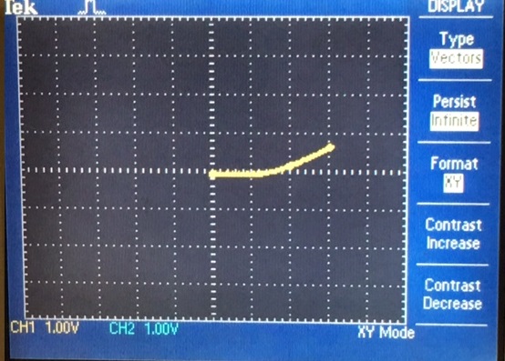
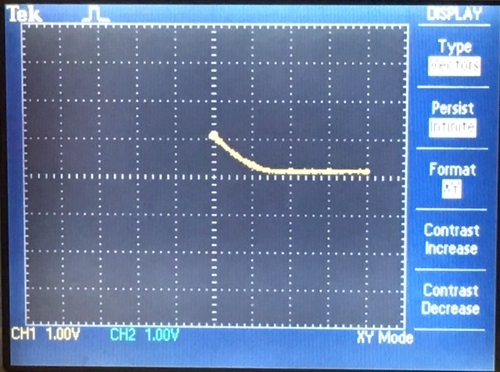
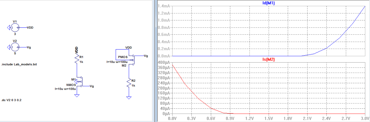
For part 1 of the experiment we have
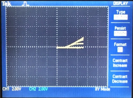
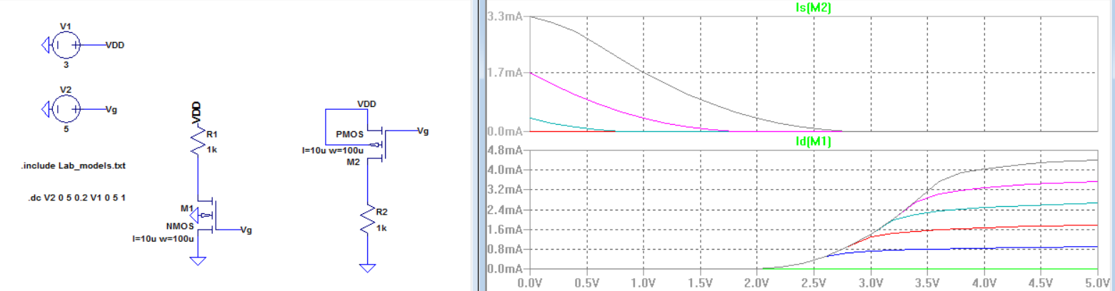
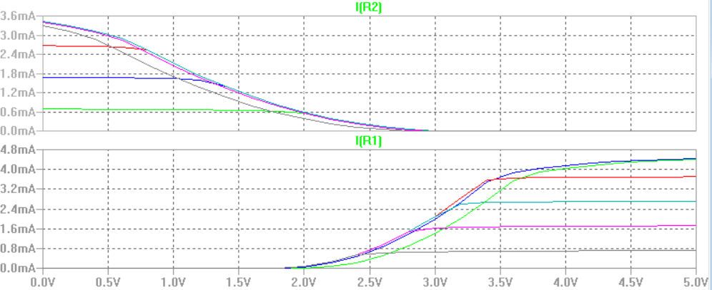
For part 2 we sweep VDS and VGS
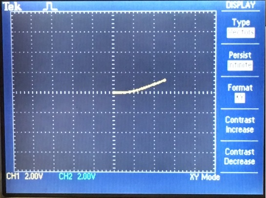
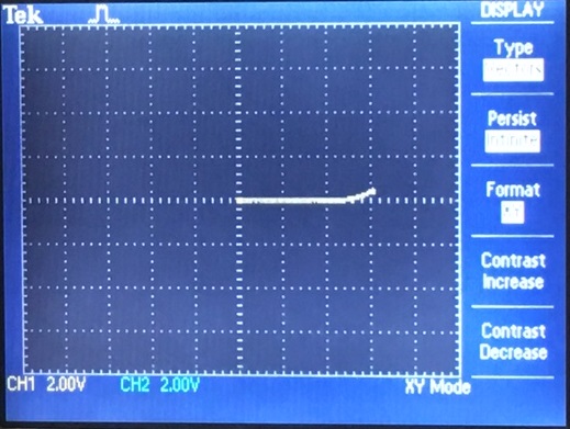
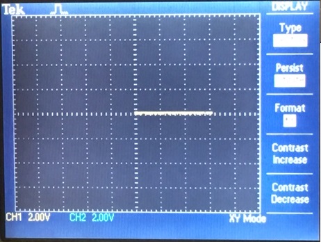
Here we see that in the nmos case the circuit starts out with no
current flow, but as VGS raises we see more current flow until the plot
stays in the triode region at higher VGS values. For the pmos there is
an inverse effect, where the circuit starts out on at low VGS but
begins to slowly turn off at highter VGS.
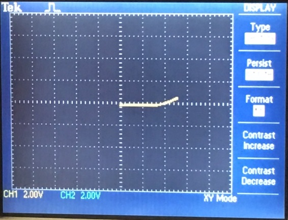
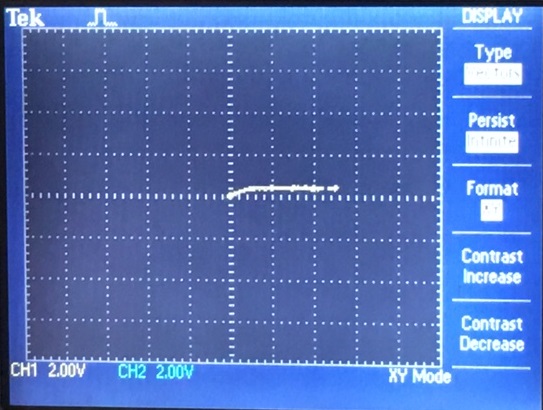
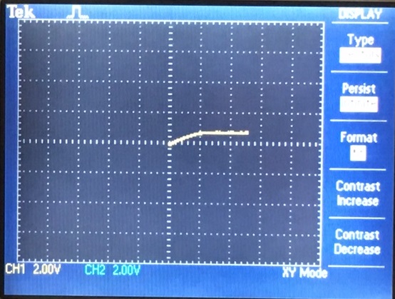
In part 3 we measure the body effect of our transistors
Here we see that as VSB and VBS becomes larger the greater the
threshold voltage becomes. Once again we see an inverse effect
relationship with the pmos.
| nmos | pmos |
 |  |
For part 2 we sweep VDS and VGS
| nmos | pmos |
 | 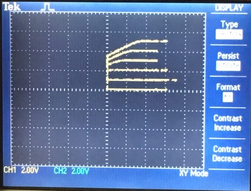 |
In part 3 we measure the body effect of our transistors
| nmos | pmos |
 |  |
 |  |
 |  |
 |  |
- Assuming that the length of the NMOS is 5 um and its width is 500 um calculate the oxide thickness if Cox (= C'ox*W*L) = 5 pF.
Cox' = Cox/ W * L = 5pf / (5um * 500 um) = 2 f F/ um^2
- From this measured data create a Level = 1 MOSFET model with (only) parameters: VTO, GAMMA, KP, LAMBDA, and TOX.
tox = Eox / Cox' = (8.85 * 3.9 )aF/um / 2fF = 0.017257 um = 17.257 nm
From page 139 we get
GAMMA = (2qEsi *NA)^1/2 / cox' = (2 * q * 11.7 * 8.85 aF/um * 10^16 )^1/2 / 2 fF/um^2 = 0.2878 V^1/2
VTO_N = 2 V
VTO_P = 2.1V
un and up values assume room tempreture.
Kpn = un * cox' = 1400 cm^2/Vs * cox' = 280 u A/V
Kpp = up * cox' = 470 cm^2/Vs *cox' = 94 u A/V
LAMBDA = 1/L * dXdl / dVDS = 1 / ID, SAT * ro
Since we lack L and the depletion layer width we cannont use the first equation. We can use the second equations to find LAMBDA however with the current measurements we find that ro is about 0, we will need to make more measurements to get an accurate value for ro.
- Compare the experimentally measured data above (the 3 plots) to LTspice-generated data (again, 3 plots) and adjust your model accordingly to get better matching.
Part 1 simulations
The plots in our simulations matches the measured curves.
Part 2 Simulations
Once again we mirror the plots shown from the measured curves. However
the current for the pmos is inverted. This due to how spice defines
current flow in transistors.
Part 3 simulations
Part 3 simulations
As we sweep VSB and VBS we see that the saturation
curve begins to shift. This is due to the body effect increasing the
threshold voltage.
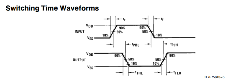
- Experimentally, similar to what is seen on the datasheet (AC test circuits seen on page 3 of the datasheet), measure the delay of an inverter using these devices (remember the loading of the scope probe is around 15 pF and there is other stray capacitance, say another 10 pF).
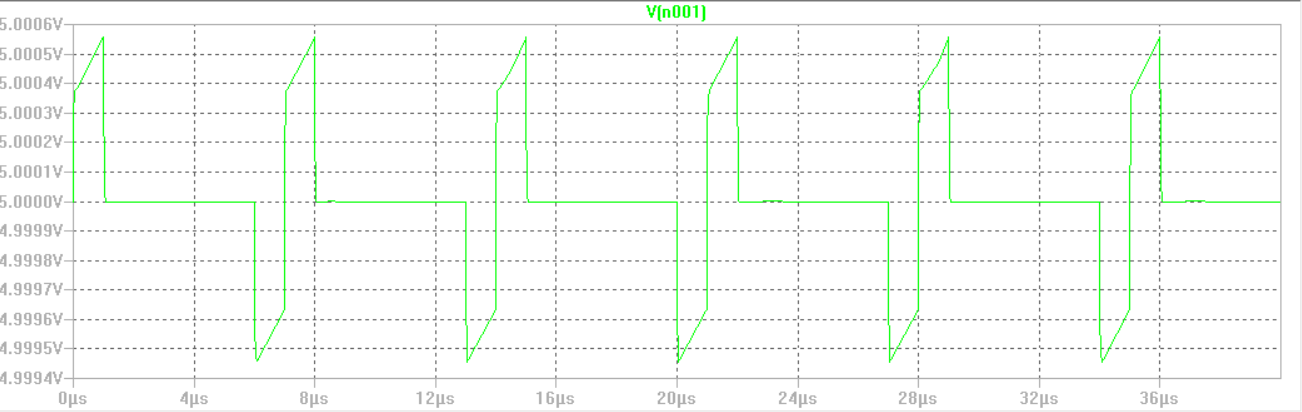
There was an issue with creating a pulse waveform, Though we see that
there is a VDD and VSS slope with our waveform.
- Using your model simulate the delay of the inverter and compare to measured results. Adjust your SPICE model to get better matching between the experimental data and the measured data.
Repeat the above steps for the PMOS device where VDS, VGS, and VSB are
replaced with VSD, VSG, and VBS respectively.