Lab 3 - EE420L
Authored
by Rodolfo Gutierrez
gutie284@unlv.nevada.edu
2/12/2016
Op-amps I, basic topologies, finite gain, and
offset
- Knowing
the non-inverting input, Vp, is at the same potential as the inverting
input, Vm, (called the common-mode voltage, VCM) what are the maximum
and
minimum allowable common-mode voltages?
- Support your
answer with an entry from the electrical characteristics table in the
datasheet.
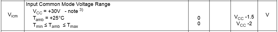
We
know from the datasheet that the VCM cannot exceed Vcc-1.5 volts for
ambient temperatures. We also know that Vcc maximum voltage is 30 V
VCM = 30 - 1.5 = 28.5 V.
So our range for VCM will be 0 V to 28.5 V
- What
is a good estimate for the op-amp's open-loop gain?
- Support your answer with a
plot from the datasheet and an entry from the electrical
characteristics table.
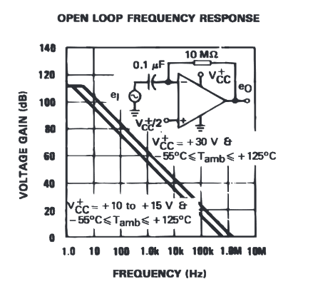
By looking at the voltage gain vs frequency graph we can tell that the gain is 100 db
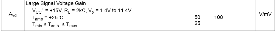
From the large signal voltage gain data we see that the gain is 100 V/mV. Where 100 V / 1x10^-3 V = 100000 V/ V
- What is a good estimate for the offset
voltage?
- For worst case design what value would
you use?
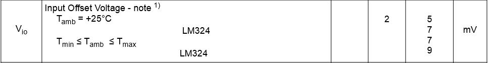
We
see that for room temperature the offset voltage will be 7 mV. For
high temperature the offset voltage will increase to 9 mV.
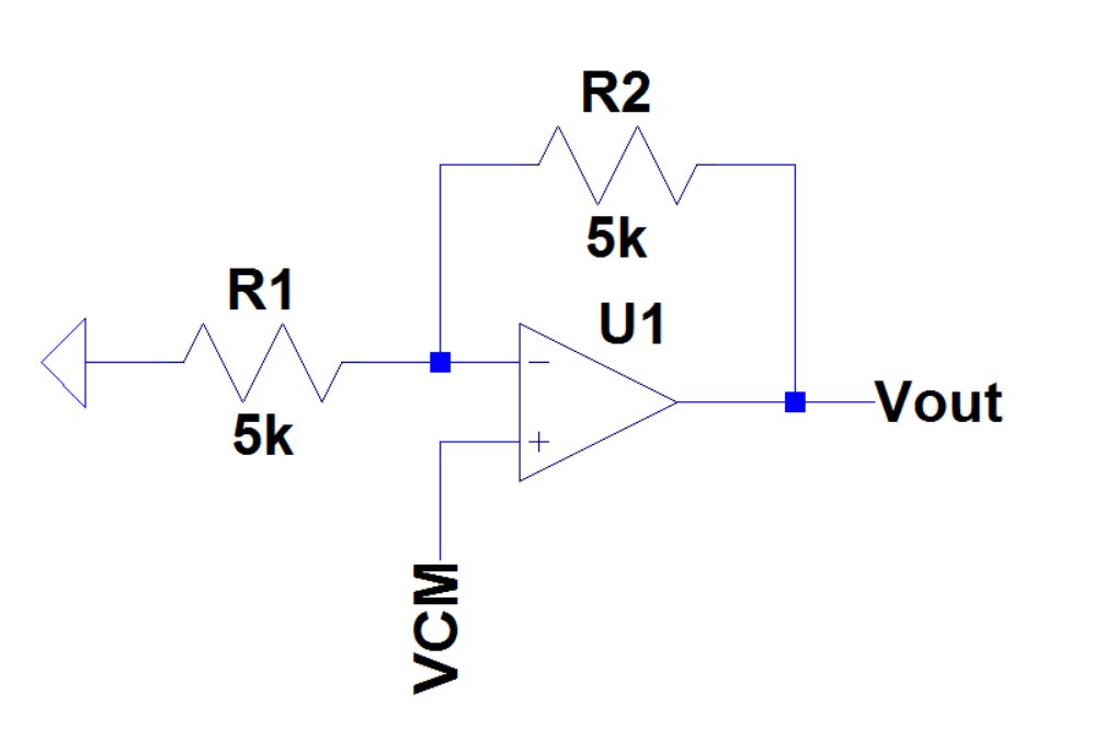
Build,
and test, the following circuit. Note that a precise value for the 5k
resistors isn't important. You can use 4.7k or a 5.1k
resistors.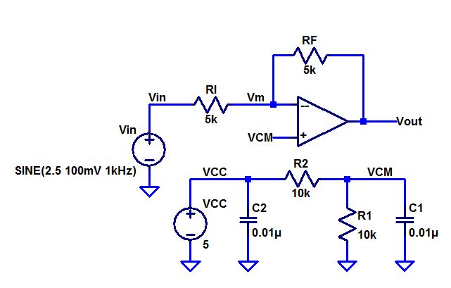
- What is the common-mode voltage, VCM? Does VCM change? Why
or why not?
We see that for DC the capacitors becomes opens, which leaves us with a voltage divider circuit.
VCM = VCC * R1 / R1 + R2
Since R1 = R2 our VCM will be VCC / 2 = 5 / 2 = 2.5 V
Unless VCC is changed then VCM will remain as 2.5 V
- What is the ideal closed-loop gain?
For
this circuit we see that RI is equal to RF in a inverting op-amp
topology. For AC we can set VCM as ground enabling us to calculate the
gain
(Vin - 0) / RI = (0 - Vout)/RF
Vout/Vin = - RF/RI = -1
So for this experiment we can expect a sinewave signal for our output but at a 180 degree phase shift away from our input.
- What is the output swing and what is it centered around?
- What
happens if the input isn't centered around around VCM, that is, 2.5
V?
- Provide a detailed
discussion illustrating that you understand what is going on.
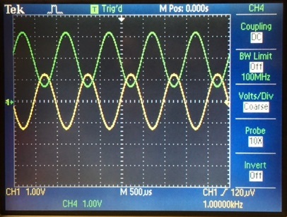
We know from our ideal closed-loop gain calculations that the output will swing at the amplitude of our input.
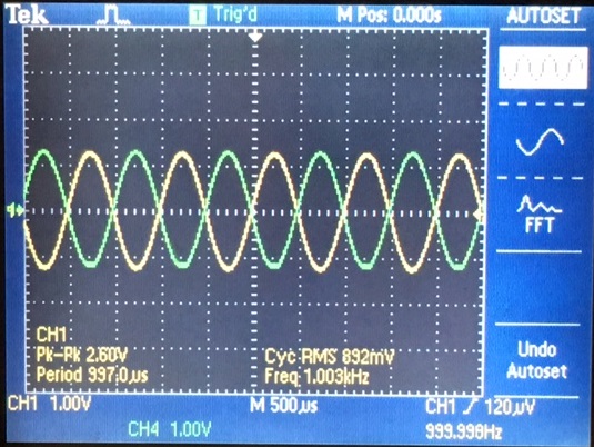
By
setting out scope to AC coupling we are able to see only the AC
effectings for our output. Our measurments confirms that the output
will be equal to the input but at a 180 degree shift.
If the input isn't centered around VCM then the output AC signal will change according to the value of our input.
However we cannot ignore the DC effects for our output.
We see that Vin becomes grounds. In the ideal op-amp case we can calculate the DC value for Vout
(0 - VCM) / R1 = (VCM - Vout) / R2
R1 = R2
- VCM = VCM - Vout
Vout = 2 * VCM
Vout = 5V when VCM = 2.5 V
However
when we had our Vcc set to 5 volts our output signal results in zero AC
signal. By reducing our Vcc we where able to get our expecting output
values.
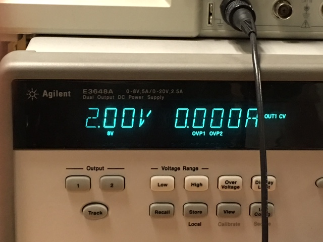
By setting our VDD to 2 volts we are able to get a output signal. At
VCM = 1 volt we see that Vout has been raised by exactly 2 volt as
comparied to our Vin. Confirming our DC calculations.
- What is the maximum allowable input signal amplitude? Why?
Our output voltage cannot exceed the supply voltage of 5 V. Using our previous calculations for both AC + DC components
of Vout we see that when VCM is 2.5 V our Vout caps out at 5V.
With a
gain of 1 we can only have an input signal of 2.5 V.
- What is the maximum allowable input signal if the magnitude
of the gain is increased to 10? Why?
We
reduce the maximum input signal to 250 mV. Now that the gain has been
increased to 10 we must reduce our input voltage so that our output =
2*VCM*10 = 5 V
- What is the point of the 0.01 uF capacitors from VCC and
VCM to ground?
- Are these values critical or could 0.1 uF, 1,000 pF, 1
uF, etc. capacitors be used?
Since
VCC and VCM are DC signals the capacitors act like opens thus
they have no effect on the circuit. The values of the capacitors are irrevelant so we can interchange them without consequence.
- The data sheet shows that this op-amp has an input bias
current that flows out of the op-amp's inputs of typically 20 nA.
- This current flows out of both the non-inverting and
inverting inputs through the resistors connected to these inputs.
- Show how the operation of the circuit can be effected if,
for example, R1 and R2, are much larger. Explain what is going on.
The
20 nA will flow through the resistors R1 and R2 which in turn reduce
our VCM value. We see that voltage created by the bia current is
20 nA * R1 // R2 = 20 nA * 10k // 10k = 20 nA * 5k = 100 uV
100 uV will not have significant impact to our VCM. However for an increased resistance of say 10 MEG we have
20nA * 5MEG = 0.1 V
This will cause a noticable reduction to our VCM which will cause our Vout DC value to be reduced.
- What is the input offset current? What does this term
describe?
It is the difference between the currents in the inverting and non-inverting terminals of the op-amp.
Explain how the
following circuit can be used to measure the op-amp's offset voltage.
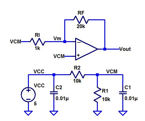
- Note that if the output voltage is precisely the same as
VCM then the op-amp has no offset voltage (this is very possible).
- To measure small offset voltages increase the gain by
increasing RF to 100k or larger. Explain what is going on.
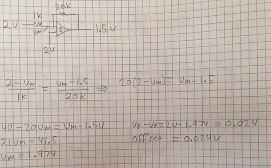
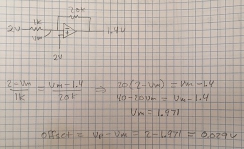
Assuming that Vm = VCM
(VCM - VCM)/1k = (VCM - Vout) / 20k
0 = (VCM - Vout) / 20k
Now for this equation to be true Vout must equal VCM. However if Vm does not equal VCM then Vout will not equal VCM.
With
this all we have to do is measure VCM and Vout. If there is a different
between VCM and Vout then we will know that the op-amp has an offset
voltage.
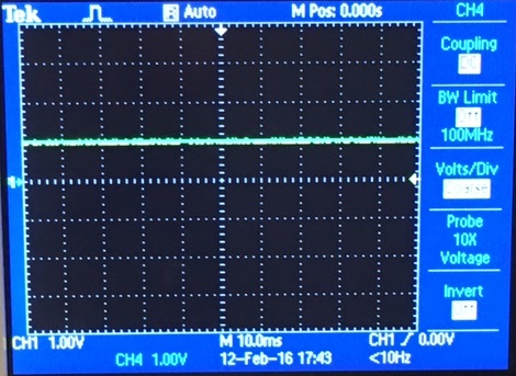
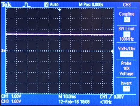
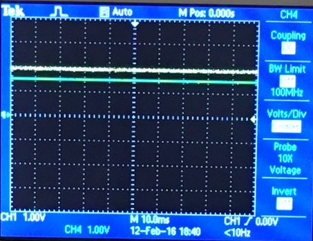
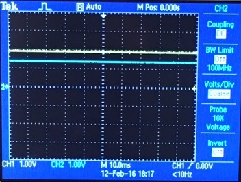
- Measure the offset voltage of 4 different op-amps and
compare them.
LM324
LM393
LM351
TL082
Return