Lab 9 - EE 420L
Author: Dane Gentry
Email: gentryd2@unlv.nevada.edu
April 20, 2016
Design of a Beta-Multiplier Reference (BMR) using the CD4007 CMOS transistor array
Click on any picture for its full size!
Pre-lab work
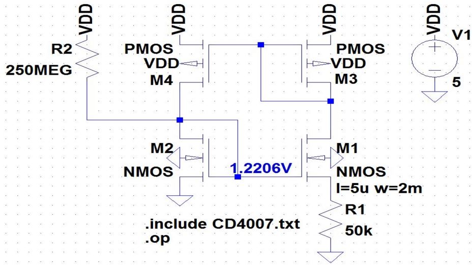
- This lab will use the level=1 MOSFET model created in lab 8 and, again, the MOSFETs in the CD4007.pdf CMOS transistor array.
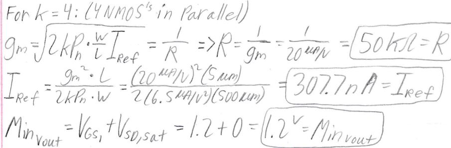
- Design and simulate the operation of a BMR that biases the NMOS devices so that they have a gm of 20 uA/V
- Use a simple (big) resistor to VDD for the start-up circuit (explain how the addition of a resistor ensures start-up).
- When
the BMR is operating the current in the big resistor should be much
smaller than the current flowing in each branch of the BMR
- Write-up,
similar to a homework assignment, your design calculations and
simulation results. (This will count as the pre-lab quiz.)
- Ensure that you show the following in what you turn in:
- Hand calculations
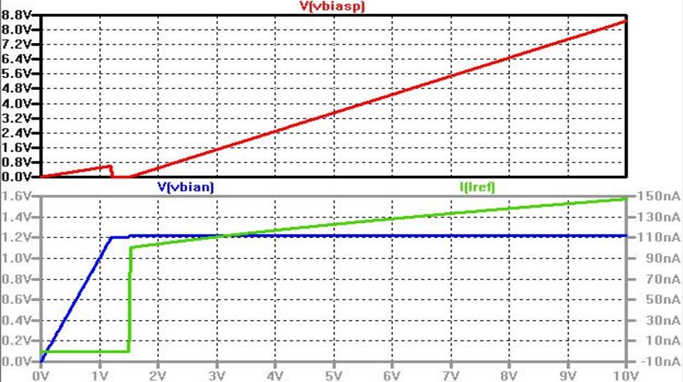
- Operation as VDD is swept from 0 to 10 V
- Vbiasn
should stabilize (be constant) after VDD hits a minimum value (estimate
this value of VDD assuming VGS/VSG is a threshold voltage and
VDS,sat/VSD,sat is zero).
- Vbiasp should follow VDD after VDD hits a minimum value (show this in simulations)
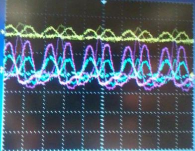
- Unstable operation if too much capacitance is shunting the BMR's resistor (see bottom of page 630)
- Comments comparing the hand calculations with the simulation results
Hand Calculations


Schematic
Simulations
Lab Description
- Learn
and experience how to characterize a BMR design using the transistors in the CD4007, then use the BMR to bias NMOS & PMOS current mirrors as well as measure the current.
Lab Requirements
In this lab you may need to use two,
or more, CD4007 chips from the same production lot (see date code on
the top of chip) to ensure using a BMR to bias a current mirror is
possible. If the CD4007 chips are not from the same production lot they
will not "match" so current mirrors will not be possible.
- Build your BMR design and characterize it as you did in the pre-lab
- You
expect the BMR to become unstable if there is a large capacitance
across the resistor, such as a scope probe (important), so care must be
exercised
- Use your BMR to bias, and thus create, a:
- NMOS current mirror
- PMOS current mirror
- Measure how the current varies through each current mirror as the voltage across the mirror changes.
- Of
course the current in the NMOS (PMOS) current mirror goes to zero as
the voltage on the drain of the output device moves towards ground (VDD)
- Using these current mirrors drive two gate-drain connected transistors
- For the first experiment use the NMOS current mirror to drive two PMOS gate-drain connected devices.
- Use
the voltages on the gate-drain connection of the two devices to bias a
cascode current mirror (characterize this mirror as before)
- For the second experiment switch, that is, use the PMOS current mirror to drive two NMOS gate-drain connected devices.
- Again, use these two voltages to bias an NMOS cascode current mirror then characterize.

Experiment 1: BMR Characterization
The table below shows the corresponding voltage values of Vbiasn and Vbiasp for VDD swept from 0 to 10 volts.
| VDD (V) | Vbiasn (V) | Vbiasp (V) |
| 0 | 0 | 0 |
| 1 | 0.81 | 0.38 |
| 2 | 0.99 | 0.67 |
| 3 | 1.09 | 1.45 |
| 4 | 1.15 | 2.46 |
| 5 | 1.18 | 3.44 |
| 6 | 1.20 | 4.57 |
| 7 | 1.22 | 5.63 |
| 8 | 1.24 | 6.57 |
| 9 | 1.25 | 7.69 |
| 10 | 1.26 | 8.49 |
The
simulations above closely agree with the table above for corresponding
voltage values of Vbiasn and Vbiasp for VDD swept from 0 to 10 volts.
The experimental measurements of Vbiasn shows that it stabilizes to a
constant value of approximately 1.5 V while the simulated Vbiasn
completely stabilizes to a constant value of 1.2 V after VDD reaches 1
V. Experimental and simulated values of Vbiasn closely agree as they
both increase with increasing VDD until they reach approximately 8.5 V
for VDD = 10 V. Any discrepancies between the experimental and
simulated results of the values for Vbiasn and Vbiasp can most likely
be attributed to the chips coming from different production lots.
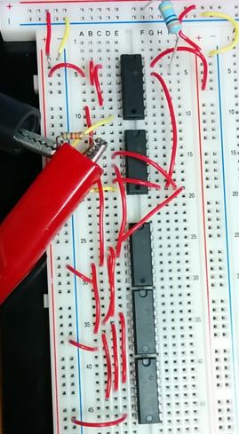
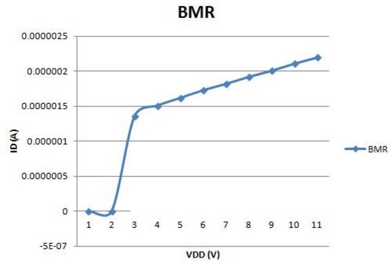
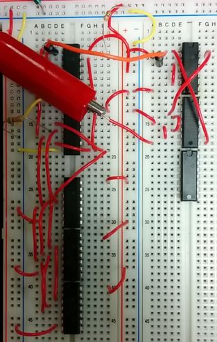
The
experimental data measured from the breadboard circuit below was used
to generate a plot (shown below) of VDD vs. ID for the BMR.
| Stable circuit (without BIG capacitor) | Unstable circuit (with BIG capacitor) |
 |  |
Experiment 2: NMOS/PMOS Current Mirror
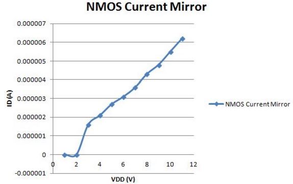
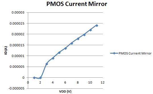
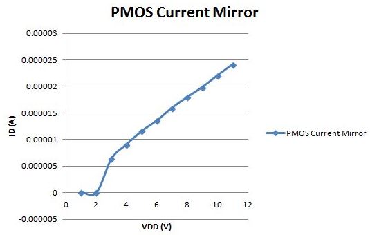
The experimental data measured from the breadboard circuit below was used to generate a plot (shown below) of VDD vs. ID for both NMOS/PMOS current mirrors.
Experiment 3: NMOS/PMOS Cascode
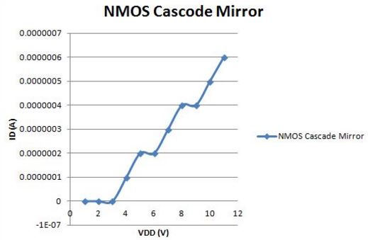
The experimental data measured from the breadboard circuit below was used to generate a plot (shown below) of VDD vs. ID for both NMOS/PMOS cascodes.

Lab Conclusion
This
lab demonstrated the design, building, and testing of a BMR using the transistors in the CD4007. An NMOS
& PMOS current mirror were also built using the biasing of the BMR,
and the current through the circuit was measured. The
experiments in this lab provided excellent experience in how
to design, build, and utilize a BMR to bias NMOS and PMOS current mirrors, and all
experiments in this
lab were performed with little difficulty and few encountered problems.
Return to EE 420 Labs