Lab 8 - EE 420L
Author: Dane Gentry
Email: gentryd2@unlv.nevada.edu
April 13, 2016
Characterization of the CD4007 CMOS Transistor Array
Click on any picture for its full size!
Pre-lab work
- Review the datasheet for the CD4007.pdf CMOS transistor array.
- Ensure
that you understand how the bodies of the NMOS are tied to pin 7 (VSS,
generally the lowest potential in the circuit, say ground) and that the
bodies of the PMOS are tied to pin 14 (VDD, generally the highest
potential in the circuit, say + 5V).
Lab Description
- Learn
and experience how to characterize the transistors in the CD4007
by building a circuit on the breadboard in order to generate various
plots related to ID, VGS/VSG, and VDS/VSD for the NMOS/PMOS
devices.
Lab Requirements
In
this lab you will characterize the transistors in the CD4007 and
generate SPICE Level=1 models. Assume that the MOSFETs will be used in
the design of circuits powered by a single +5 V power supply. In other
words, don't characterize the devices at higher than +5 V voltages or
lower than ground potential.
- Experimentally generate, for the NMOS device, plots of:
- ID v. VGS (0 < VGS < 3 V) with VDS = 3 V
- ID v. VDS (0 < VDS < 5 V) for VGS varying from 1 to 5 V in 1 V steps, and
- ID v. VGS (0 < VGS < 5 V) with VDS = 5 V for VSB varying from 0 to 3 V in 1 V steps.
- Note
that for this last one, if VSS (NMOS body) is ground (again, the
Body, VB, is grounded) then the source voltage will be varied from 0 to
3 V in 1 V steps to realize VSB ( = VS - VB = VS) varying from 0 to 3 V
in 1 V steps. At the same time VGS will be varied from 0 to 3 V (when
VS = 0), 1 to 4 V (when VS = 1 V), 2 to 5 V (when VS = 2 V), and 3
to 5 V (when VS = 3 V). In other words, as VS is increased by 1 V the
VGS has to shift up by 1 V as well.
- Assuming
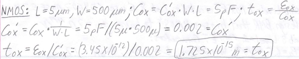
that the length of the NMOS is 5 um and its width is 500
um calculate the oxide thickness if Cox (= C'ox*W*L) = 5 pF.
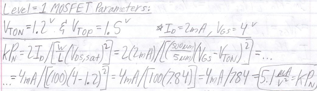
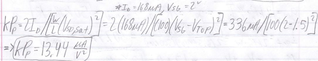
- From this measured data create a Level = 1 MOSFET model with (only) parameters: VTO, GAMMA, KP, LAMBDA, and TOX.
- Compare
the experimentally measured data above (the 3 plots) to
LTspice-generated data (again, 3 plots) and adjust your model
accordingly to get better matching.
- Experimentally,
similar to what is seen on the datasheet (AC test circuits seen on page
3 of the datasheet), measure the delay of an inverter using these
devices (remember the loading of the scope probe is around 15 pF and
there is other stray capacitance, say another 10 pF).
- Using
your model simulate the delay of the inverter and compare to measured
results. Adjust your SPICE model to get better matching between the
experimental data and the measured data.
- Repeat the above steps for the PMOS device where VDS, VGS, and VSB are replaced with VSD, VSG, and VBS respectively.
For the following questions and experiments assume VCC+ = +5 Volts
NMOS:
| Experiment 1 (100 Ohm Sampling Res) | 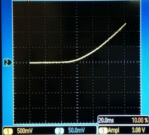 |
Experiment 2 (200 Ohm Sampling Res)
VGS = 1V | 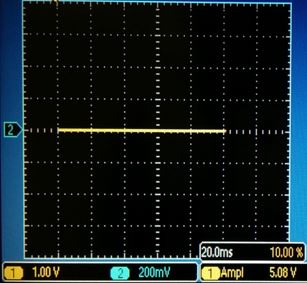 |
Experiment 2 (200 Ohm Sampling Res):
VGS = 2V | 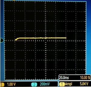 |
Experiment 2 (200 Ohm Sampling Res):
VGS = 3V | 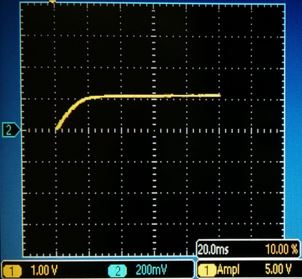 |
Experiment 2 (200 Ohm Sampling Res):
VGS = 4V | 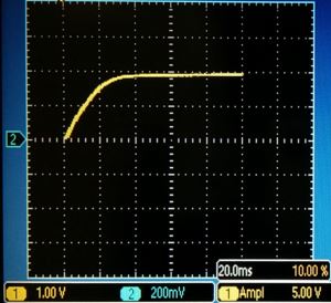 |
Experiment 2 (200 Ohm Sampling Res):
VGS = 5V | 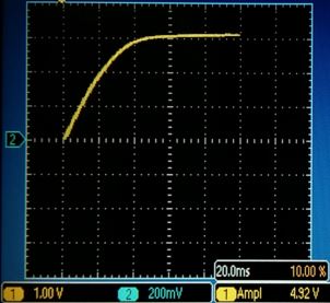 |
Experiment 3 - Varying VSB from 0 to 3V
(Plot generated from measuring voltage across 200 Ohm sampling res) | 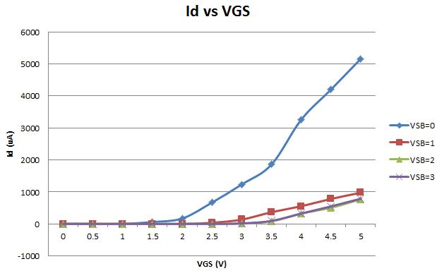 |
Simulations:
| Experiment 1 | 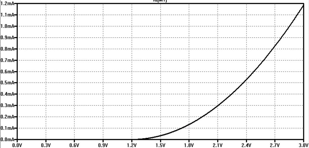 |
| Experiment 2 | 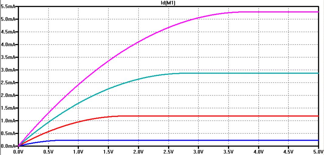 |
| Experiment 3 | 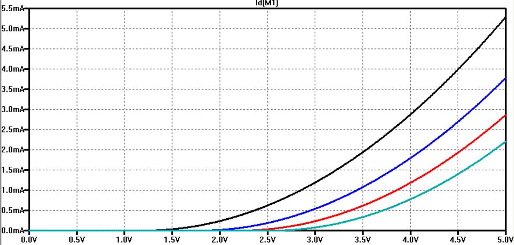 |
Simulations and experimental results all agree.
PMOS:
| Experiment 1 (100 Ohm Sampling Res) | 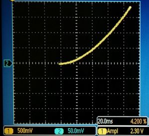 |
Experiment 2 - VSG varied 1 to 5V
(Plot generated from measuring voltage across 200 Ohm sampling res) | 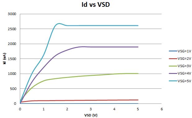 |
Experiment 3 - Varying VBS from 0 to 3V
(Plot generated from measuring voltage across 200 Ohm sampling res) | 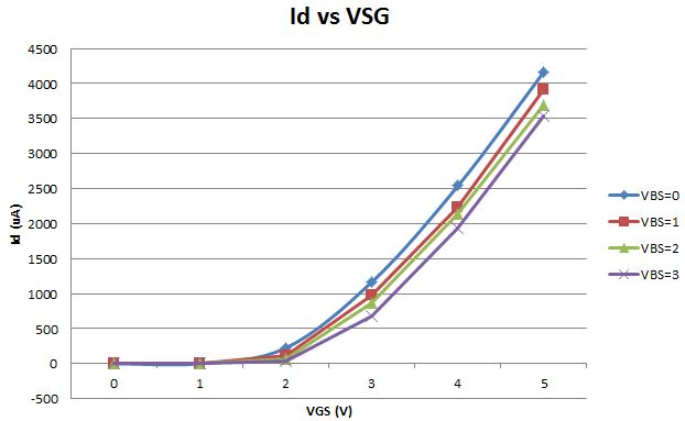 |
Simulations:
| Experiment 1 | 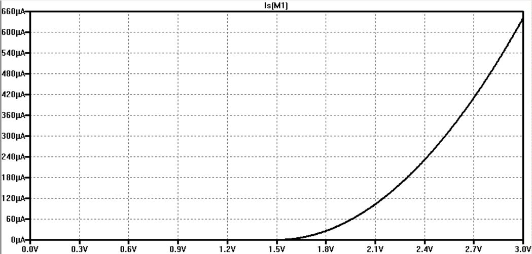 |
| Experiment 2 | 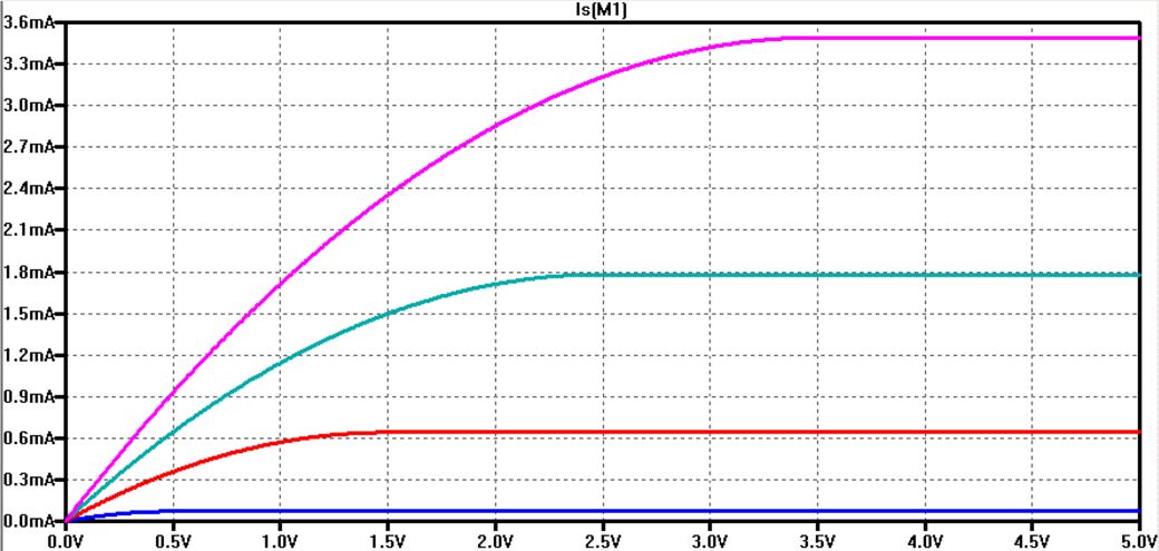 |
| Experiment 3 | 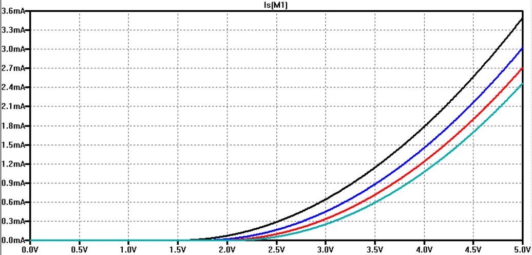 |
Simulations and experimental results all agree.
Hand Calculations:

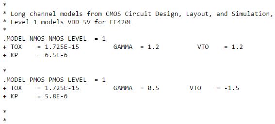
Basic Level=1 MOSFET Model:
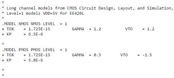
The
above Level = 1 MOSFET model with parameters VTO, GAMMA, KP, LAMBDA,
and TOX was created in Spice based on the measured experimental data.
The
model parameters were adjusted (seen below) in order to provide better
matching between experimental results and Spice simulations.
Modified Basic Level=1 MOSFET Model:
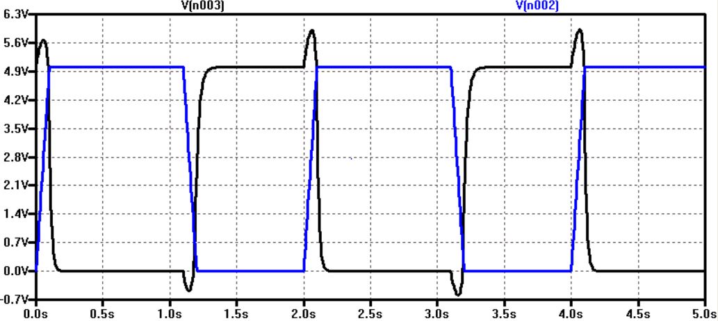
Inverter Experiment:
Simulation Results
Lab Conclusion
This
lab demonstrated how to characterize the transistors in the CD4007
by building a circuit on the breadboard in order to generate various
plots related to ID, VGS/VSG, and VDS/VSD for the NMOS/PMOS devices.
The plots were compared to simulations which closely agree. Model text
files were created for the CD4007 for specific parameter values in
Spice including VTO,
GAMMA, KP, LAMBDA, and TOX. These parameters were adjusted for better
matching between experimental and simulated results. Finally, an
inverter was designed, built, and tested utilizing the devices
in the CD4007, and the delay was measured and compared to simulated
results. Overall, the
experiments in this lab provided excellent experience surrounding
transistor arrays in the CD4007 and the operation of its devices. All
experiments in this
lab were performed with little difficulty and few encountered problems.
Return to EE 420 Labs