Lab 5 - EE 420L
March 9, 2016
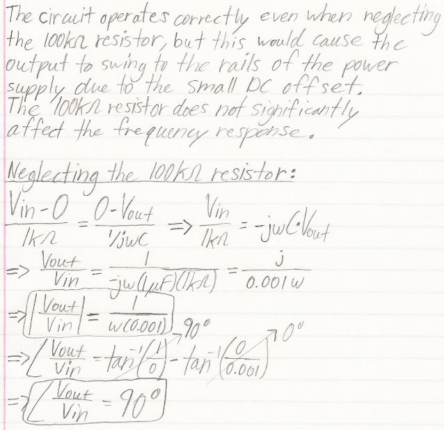
Hand Calculations and Explanation
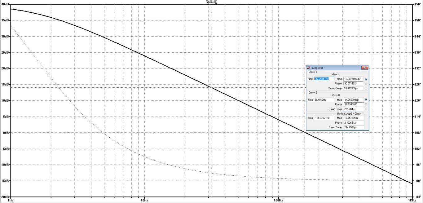
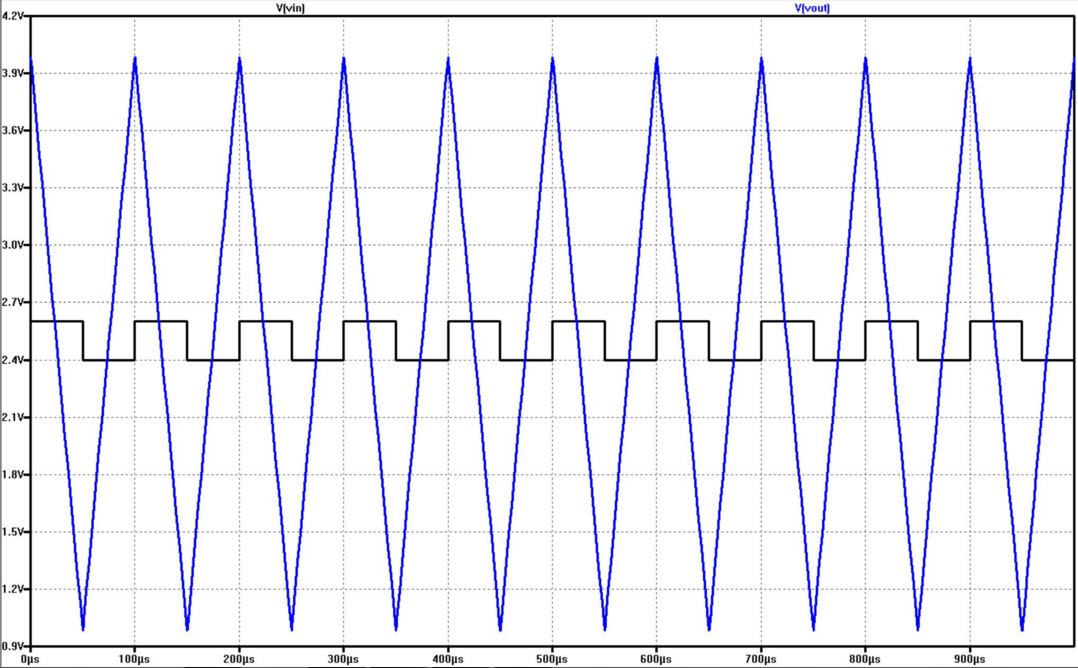
LTspice Schematic LTspice Simulation (Ft = 157 Hz)

Part 2:
Experimental Results
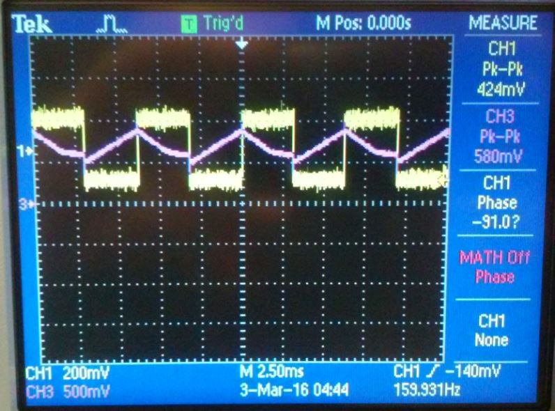
Sinusoidal Signal (Ft = 159 Hz) Square Wave Signal (Ft = 159 Hz)
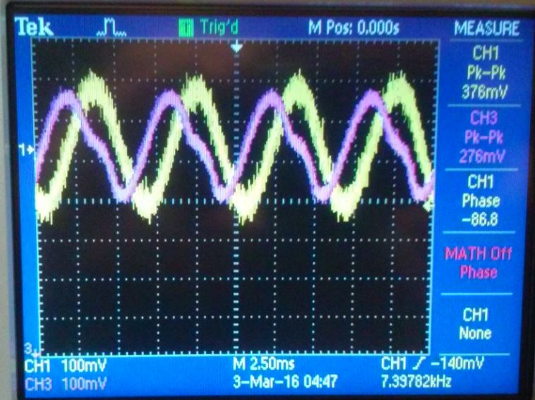
The calculated unity-gain frequency is Ft = 159 Hz. The sinusoidal signal shown above displays input and output signals with peak values that
are approximately equal. The square wave signal shown above, however, displays an output (triangle wave) that has a peak value greater than
the input (notice the different voltage scales). The two peak values for the square wave signal are nonetheless the same order of magnitude.
In addition, both of the images above display an approximate 90 degree phase shift as expected from the hand calculations.
Part 3:
Hand Calculations

LTspice Schematic LTspice Simulation
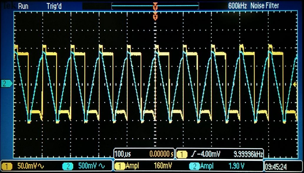
Experimental Results
Conclusion
The triangle-wave output did not get as close to the power supply rails as expected, most likely due to manufacture defects/inconsistencies
or other flaws in the op amp. It is noted that in order to avoid an excessive DC offset, the 2.5 Vm voltage must be very close to the 2.5 Vin voltage.
By using a smaller capacitor value and thus calculating a higher value for the resistor, the swing of the output could theoretically increase.
Lab Conclusion
This lab demonstrated the operation and use of op-amp integrators, specifically in integrating a square wave input signal in order to produce a triangle-wave
output. The experiments in this lab provided excellent experience in how to design, build, and utilize an integrator to produce a triangle wave output from a
square wave input, and all experiments in this lab were performed with little difficulty and few encountered problems.