Final Project - EE 420L
Author: Dane Gentry
Email: gentryd2@unlv.nevada.edu
May 4, 2016
Design of a Transimpedance Amplifier (TIA)
Click on any picture for its full size!
Project Description
- Learn
and experience how to design, simulate, build, and test a transimpedance amplifier (TIA).
Project Requirements
For this project, we are required to design, simulate, build, and test a transimpedance amplifier (TIA) using ZVN3306A or ZVP3306A (or both) MOSFETs and as many resistors and
capacitors as necessary with a gain of 30k. We are required to get the
fastest possible design driving a 10k load with the larget possible
output swing. AC coupling input and output is okay as long as the
design can pass a 100Hz input current.
These requirements are detailed below:
- Use ZVN3306A or ZVP3306A (or both) MOSFETs
- Use as many resistors and capacitors as necessary with a gain of 30k
- Get the fastest possible design driving a 10k load with the larget possible output swing
- AC coupling input and output is okay as long as the design can pass a 100Hz input current
Design Considerations
The
push-pull amplifier introduced in Lab 6 is used as a general topology
for the design of the transimpedance (TIA) amplifier. In addition, the
transconductances of the ZVN3306A (NMOS) and ZVP3306A (PMOS) (gmn and gmp, respectively)
are used from Lab 6 and are also verified using the Spice error log in
the TIA schematic below. Rs is set as 1k (increasing this resistance
decreases the current through it), C1 is set as 10uF, R1 is set as 40k
(this resistance determines the gain of the TIA, and a resistor value
of R1=40k was used to slightly increase the gain) and the load is a 10k
resistor as stated in the project requirements. In addition, VDD is set
as 10V.
Hand Calculations
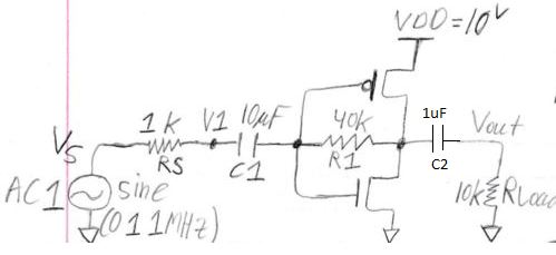
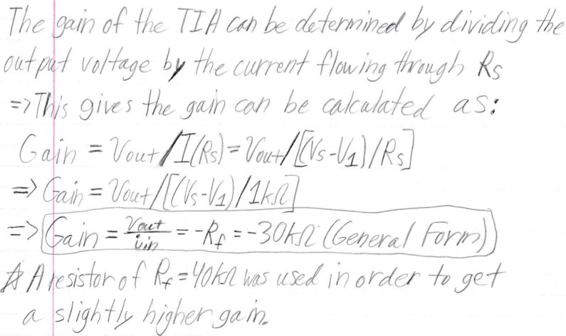
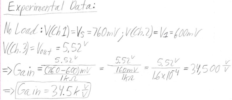
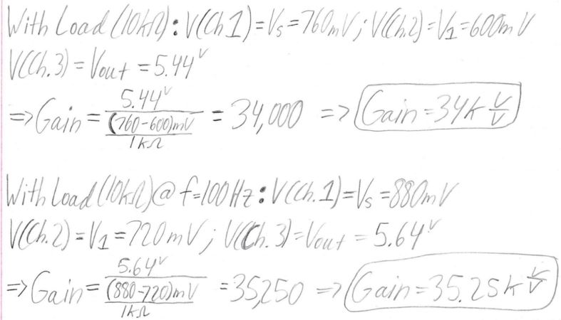
Table Summary
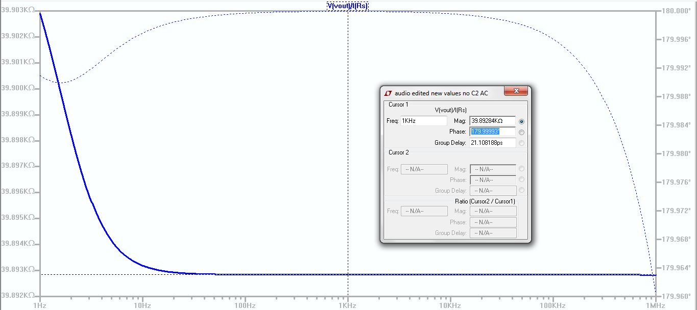
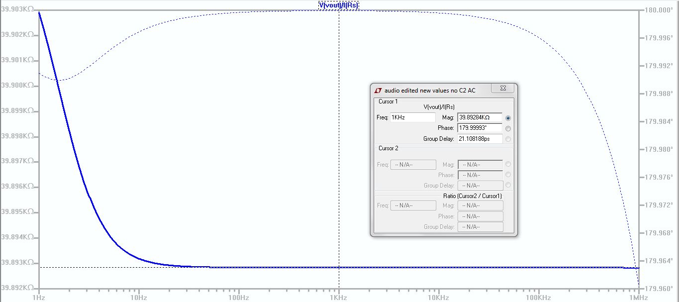
The
simulations in the table below
show the gain of the TIA by plotting the ouput voltage divided by the
current flowing throught Rs. The simulations indicate the gain of the
TIA is approximately 40k V/V with a phase of 180 degrees which agrees with -Rf=-40k. The experimental gains in the table below
are calculated in the hand calculations section above by dividing the
output voltage (CH. 3) by the current across Rs=1k. The experimental
gains in the table below are then calculated as (CH. 3)/((CH. 1 - CH.
2)/Rs). | Schematic | Simulation | Experimental |
| No Load | 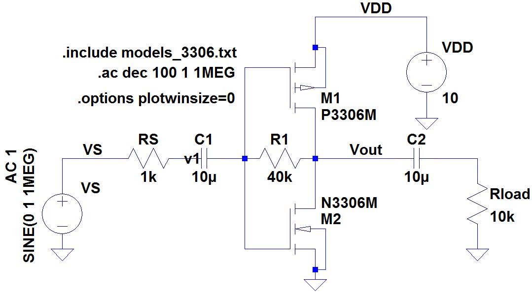
| 
Gain = 39.89k V/V | 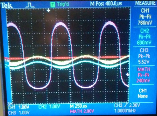
Gain = 34.5k V/V |
| With Load | 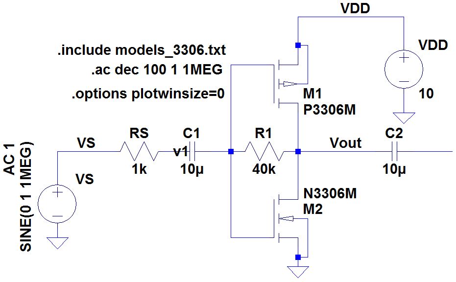
| 
Gain = 39.91k V/V | 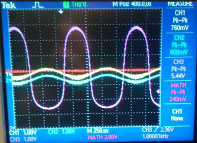
Gain = 34k V/V |
| f=100Hz With Load | 
| 
Gain = 39.91k V/V | 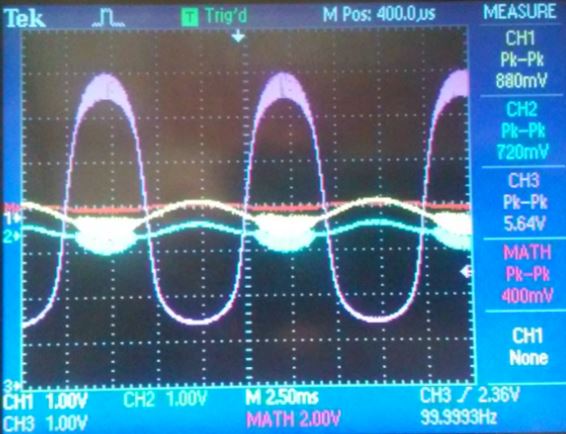
Gain = 35.251k V/V |
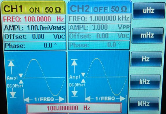
The image below shows the function generator used in this project set at a frequency of 100Hz.
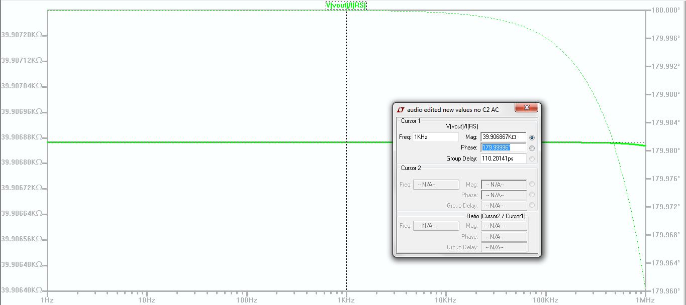
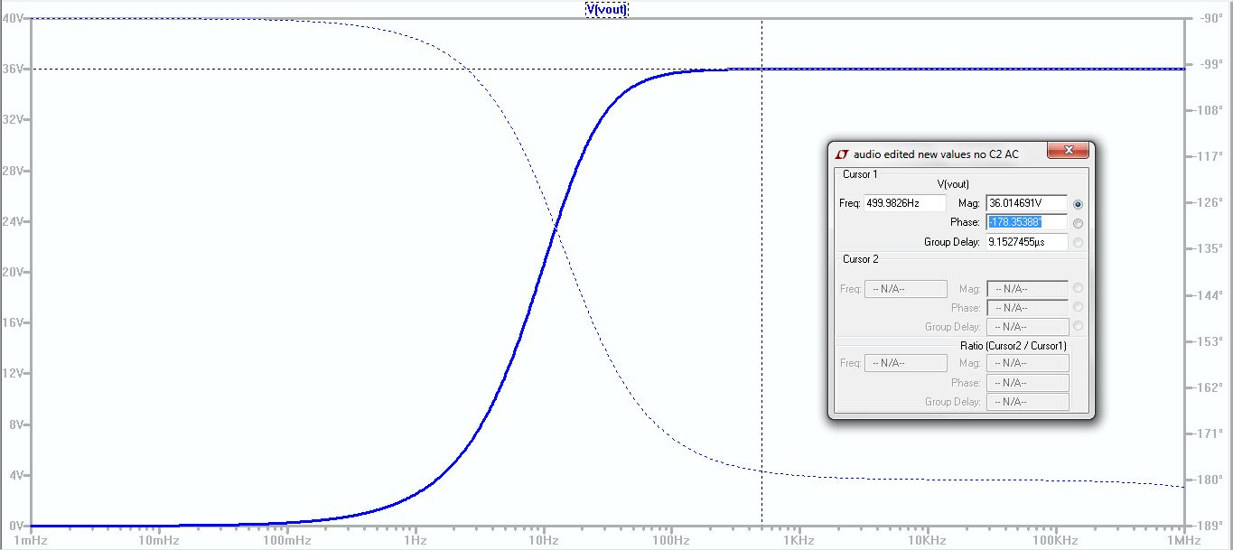
The simulation below shows the output swing of the TIA with the input signal frequency swept from 1mHz to 1MHz. The simulation indicates the output of the TIA swings from 0V (until approximately 0.001 Hz) to 36.01V (at approximately 500 KHz).
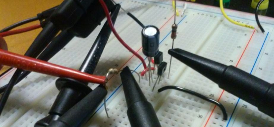
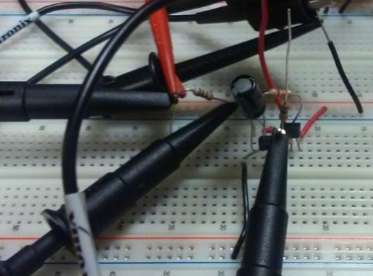
The
images below show the TIA cicuit implemented on a breadboard. The red
probe is coming from the function generator while the three black scope
probes are connected to the two nodes across Rs as well as the output
node attached to the load resistor (Rload) in order to plot these node
voltages on an oscilloscope.
Project Conclusion
This
project demonstrated the designing, simulating, building, and testing
of a transimpedance amplifier (TIA). All aspects of this project
were performed with little difficulty and few encountered problems. A
resistor value of R1=40k was used to slightly increase the gain.
The
table summary shows that the gain of the TIA does not vary
significatnly with a load attached compared to no load attached, and
the TIA is able to achieve the same gain while passing a 100Hz input
signal. Furthermore, simulated values of gain closely agree with
experimental results for values of gain.
Return to EE 420 Labs