Lab 8: Characterization of the CD4007 Array ECE 420L
Authored By: Joey Yurgelon
Email: yurgelon@unlv.nevada.edu
April 14th, 2015
Pre-lab Work:
- Review the datasheet for the CD4007.pdf CMOS transistor array.
- Ensure
that you understand how the bodies of the NMOS are tied to pin 7 (VSS,
generally the lowest potential in the circuit, say ground) and that the
bodies of the PMOS are tied to pin 14 (VDD, generally the highest
potential in the circuit, say + 5V).
Lab Description:
- Students
will characterize the transistor array and develop a spice model for use.
Lab Requirements:
In
this lab you will characterize the transistors in the CD4007 and
generate SPICE Level=1 models. Assume that the MOSFETs will be used in
the design of circuits powered by a single +5 V power supply. In other
words, don't characterize the devices at higher than +5 V voltages or
lower than ground potential.
- Experimentally generate, for the NMOS device, plots of:
- ID v. VGS (0 < VGS < 3 V) with VDS = 3 V
- ID v. VDS (0 < VDS < 5 V) for VGS varying from 1 to 5 V in 1 V steps, and
- ID v. VGS (0 < VGS < 5 V) with VDS = 5 V for VSB varying from 0 to 3 V in 1 V steps.
- Note
that for this last one, if VSS (NMOS body) is ground (again, the
Body, VB, is grounded) then the source voltage will be varied from 0 to
3 V in 1 V steps to realize VSB ( = VS - VB = VS) varying from 0 to 3 V
in 1 V steps. At the same time VGS will be varied from 0 to 3 V (when
VS = 0), 1 to 4 V (when VS = 1 V), 2 to 5 V (when VS = 2 V), and 3
to 5 V (when VS = 3 V). In other words, as VS is increased by 1 V the
VGS has to shift up by 1 V as well.
- Assuming that the length of
the NMOS is 5 um and its width is 500 um calculate the oxide
thickness if Cox (= C'ox*W*L) = 5 pF.
- From this measured data create a Level = 1 MOSFET model with (only) parameters: VTO, GAMMA, KP, and TOX.
- Compare
the experimentally measured data above (the 3 plots) to
LTspice-generated data (again, 3 plots) and adjust your model
accordingly to get better matching.
- Experimentally, similar to
what is seen on the datasheet (AC test circuits seen on page 3 of the
datasheet), measure the delay of an inverter using these devices
(remember the loading of the scope probe is around 15 pF and there is
other stray capacitance, say another 10 pF).
- Using your model
simulate the delay of the inverter and compare to measured results.
Adjust your SPICE model to get better matching between the experimental
data and the measured data.
- Repeat the above steps for the PMOS device where VDS, VGS, and VSB are replaced with VSD, VSG, and VBS respectively.
Experimental Results:
Exercise #1: MOSFET Chracterization for the NMOS
- My
partner and I started out using the XY functionality of the ocilloscope
with a triangle wave input to plot our various IV curves as we learned
in 320L. While it started out well, we did hit a wall and ended up
wasting alot of time when were should not of. We took note of the
sampling resistors used so that we could determine the current later
on. For those IV-curves with stepped values, I have decided to only
show one as it should be enough to compare between experimental and
simulated results. The tables below list our various experimental
results in the first
columns and then the simulation plots due to our developed spice model.
The developed spice model can be seen here.

Experimental NMOS Variation to VGS - Rsampling - 100 Ohms | Simulation NMOS Variation to VGS |

Exp. NMOS VDS Sweep with VGS (4V) steps - Rsampling - 200 Ohms | 
Simulation NMOS VDS Sweep with VGS steps |
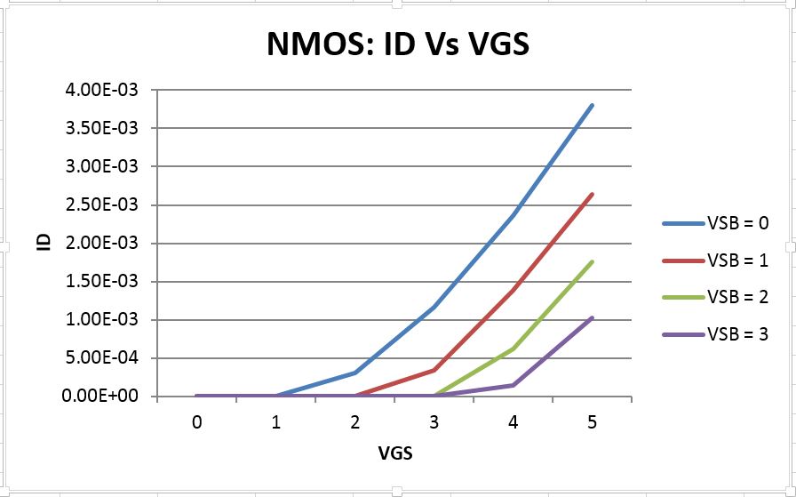
Experimental NMOS VGS Sweep with VSB Step | 
Simulation NMOS VGS Sweep with VSB Step |
Exercise #2: MOSFET Chracterization for the PMOS- These
simulations and measurements follow similar suit as that of the NMOS
version above. The left side column is all of the experimental results,
and the right side are the simulations built around the experimental
Spice model. The PMOS model ended up matching alot better than the NMOS
counterpart which was notable due to the XY measurements made earlier
that introduce some error into the system with the sampling resistor.
Again, the model can be found here.

Experimental PMOS Variation to VSG - Rsampling - 200 Ohms | Simulation PMOS Variation to VSG |

Experimental PMOS VDS Sweep with VSG steps | 
Simulation PMOS VDS Sweep with VSG steps |

Experimental PMOS VGS Sweep with VBS Step | 
Simulation PMOS VGS Sweep with VBS Step |
Exercise #3: Inverter Characterization for the Transistor Array and Spice Model
- The
values for the model were determined from our experimental results
above. These results were then used to plug into the various formulas
to find the other vital parameters for characterizing the MOSFETS.
- Tox = (Eox)/(Cox/(W*L)) = 1.725E-15m
- Vthon = 1.2V; Vthop = 1.5V
- Kp = (2*ID)/((W/L)(VDS,Sat)^2); KPn = 5.1 (uA)/(V^2); Kpp = 13.44 (uA)/(V^2)
- Gamma = -del(Vth)/(del(VBS); KPn = 1; Kpp = 0.5
- NOTE:
These parameters were changed after performing the above simulations.
There were some clear issues with the Kp value of my models, and they
were changed to fit accordingly with the simulated results. All of the
links listed in this report contain the most recent model file.
- These values were then combined to form the level = 1 Spice Model located here.

Experimental Inverter Delay/Rise/Fall Times | Simulation Inverter |
Return to EE 420L Labs


