LAB 6 - ECE 421L
Mario Valles
March 20, 2015
Single-stage
transistor amplifiers
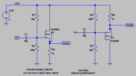
- Below are schematics for NMOS and PMOS source followers amplifiers (also known as common-drain amplifiers).
- Brief circuit description:
- This circuits are
source follower (common drain) amplifer. They both have the drain in
commmon and the output on the source. Their output should follow the
same changes on the source.
- Simulate the operation of these amplifiers.


- We can see the output of the nmos amplifier is 10mV, equal than the input.While, the pmos amplifier has 10mV also equal to the input
- Hand calculate, and then verify your hand calculations with experimentation and simulations, the gains and the input and output resistances ensuring that your test signals are at a high enough frequency that the caps have negligible impedance but not so high that the gain is dropping off.
-
- gm for NMOS
- gm for pmos
- Calculations: with gmp = 11m S and gmn = 18m
- Nmos --> Vout/Vin = 1/gm/(1/gm + R) = (1/0,018)/(1/0.018+1k) = 0.947 V/V
- Pmos --> Vout/Vin = 1/gm/(1/gm + R) = (1/0,011)/(1/0.011+1k) = 0.917 V/V
- NRin --> R1||R3 = 100k||50k = (100k*50k)/(100k+50k) = 33.3 k ohms
- PRin --> R4||R5 = 100k||50k = (100k*50k)/(100k+50k) = 33.3 k ohms
- NRout --> (1/gmn)||RL = (1/0,018)(1k)/(1/0.018+1k) =52.6
- PRout -->(1/gmp)||RL = (1/0,011)(1k)/(1/0.011+1k) =83.3
- Experiments Results were as follows
-
Gain
Nmos
Vout/Vin = 1.2 V
Pmos
Vout/Vin = 1.2 V
Rin
Nmos =
26.4k
Pmos =
34.7k
Rin=
|(Vout/Vin)RT/(1-(Vout/Vin))|
Rout
Nmos=
58.5 ohms
Pmos=
192 ohms
Rout=
|(Vout/Vin)RT/(1-(Vout/Vin))|
- In your lab report discuss, in your own words, how to measure the input resistance.
- For measuring the
input resistance we put the calculated resistance at the input, then we
measure the voltage at the input of the amplifier and at the input of
the signal. We say voltage at the amplifier to be Vout and voltage at
the signal is Vin. Then we made the following eq. Rout= (Vout/Vin)RT/(1-(Vout/Vin)this will be our input resistance.
- Again,
in your lab report discuss how to measure the
output resistance.
- The way we calculate the output resistance is by placing a big capacitor at the output and the calculated resistance in series. The put the signal at the en of the calculated resistance RT which will be Vin, and the output (Vout) at the node connecting the MOSFET source. If the calculated resistance is half then is exactly the same as RT. if not we did the following eq. for Rout --> Rout= (Vout/Vin)RT/(1-(Vout/Vin)) this will be our output resistance
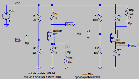
- Below are two common-source amplifiers.


- Discuss
the operation of these amplifiers in your lab report including both DC and
AC operation.
- This are common source amplifier this circuits amplify the signal input
- on DC the circuit is biased in a way to put the MOSFET in saturation mode this is done by a large enough VDD and a voltage divider in the gate also with a resistance on the drain and the source small enough to not make the transistor in triode region
- On AC the gain is calculated by dividing the resistance in the draing by the resistance in the source -->Vout/Vin = Rd/Rs
- Hand calculate the gains and the input/output resistances.
- NMOS G = Vout/Vin = -R8/(1/gmn + R2||Rsn) = -1k/(1/0.018 + 1k||100) =-6.83 V/V
- PMOS G = Vout/Vin = -R6/(1/gmp + R27|Rsp) = -1k/(1/0.011 + 1k||100) =-5.5 V/V
- NRin --> R1||R3 = 100k||50k = (100k*50k)/(100k+50k) = 33.3 k ohms
- PRin --> R4||R5 = 100k||50k = (100k*50k)/(100k+50k) = 33.3 k ohms
- NRout --> RD = 1k
- PRout -->RD = 1k
- How does the source resistance, Rsn or Rsp, influence the gain.
- Gain decreases as Rsn or Rsp increases
- Again compare your hand calculations to simulation and experimental results.
-
Gain
Nmos
Vout/Vin = 5.2 V
Pmos
Vout/Vin = 2.96 V
Rin
Nmos =
26.4k
Pmos =
34.7k
Rin=
|(Vout/Vin)RT/(1-(Vout/Vin))
Rout
Nmos=
724ohms
Pmos=
960ohms
Rout=
|(Vout/Vin)RT/(1-(Vout/Vin))|
- Below are two common-gate amplifiers.
- Discuss
the operation of these amplifiers in your lab report including both DC and
AC operation.
- This amplifier
works as the common source, but with a positive gain. The DC is apply
in way to maintain the transistor in the saturation region. The
campaictors are there as open for DC and shorts for AC, and the gate is
biased with a voltage divider
- The AC gain
is calculated by having the Rdrain/Rsource, resistance in the drain by
the resistance in the source, however, as mentioned before the gain in
here is positive as difference of the common source. It is call common
gate becuase the gate is grounded and is common to the source and drain.
- Hand calculate the gains and the input/output resistances.
- NMOS G = Vout/Vin = R8/(1/gmn + R2||Rsn) = -k/(1/0.018 + 1k||100) =6.83 V/V
- PMOS G = Vout/Vin = R6/(1/gmp + R27|Rsp) = 1k/(1/0.011 + 1k||100) =5.5 V/V
- NRin --> R1||R3 = Rsn+ 1/gmn||R2= 10+1k||1/0.018 = 152.6 ohms
- PRin --> R4||R5 = Rsp+ 1/gmp||R7= 10+1k||1/0.011 = 183.3 ohms
- NRout --> RD = 1k
- PRout -->RD = 1k
-
How does the source resistance, Rsn or Rsp, influence the gain.Gain
Nmos
Vout/Vin = 5.2 V
Pmos
Vout/Vin = 2.96 V
Rin
Nmos =
418 ohms
Pmos =
335 ohms
Rin=
|(Vout/Vin)RT/(1-(Vout/Vin))
Rout
Nmos=
980 ohms
Pmos=
1.8 khms
Rout=
|(Vout/Vin)RT/(1-(Vout/Vin))
- Increasins Rsn OR Rsp will decrease the gain
- Again compare your hand calculations to simulation and experimental results.
- We saw the data is different, we think this is due to the difference in gm and Ro of the transistors.
- Below is a push-pull amplifier.
- Discuss
the operation of this amplifier in your lab report including both DC
and AC operation.
- Hand calculate the gain of this amplifier
- id = vsg1*gmp
- id = vsg2*gmn
- vsg1 = vsg2 = vin
- vout/vin = R1(gmn+gmp)= 100k(11m+18m)=2.9k V/V
- Do you expect this amplifier to be good at sourcing/sinking current? Why or why not?
- Yes because if the
pmos is on the nmos is off and the amplifier will source current and if
the nmos is on the pmos will be off, then the amplifier will sink
current.
- What happens to the gain if the 100k resistor is replaced with a 510k resistor? Why?
- The gain increaseis because more voltage is drop across it.
- Again compare your hand calculations to simulation and experimental results.
100k
500k
Return to Mario Valles home