Final Project - EE 420L
The purpose of this final project is to design and byuild a bandgap voltage reference (BGR). We can use as many diodes, resistors and capacitors as needed, along with two CD4007 chips from the same production lot in order to ensure current mirrors are possible.
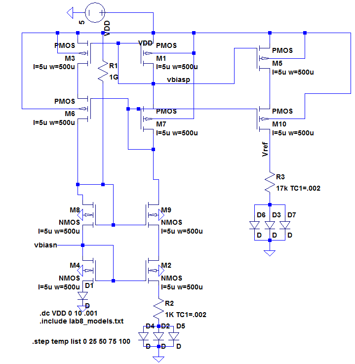
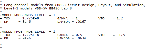
The first part of the BGR we have to design is the Current mirror. This is so that we can have the same current running through each branch. Ideally we would want to use a cascode structure in order to generate the current in the branch which we would have our Voltage Reference. In order to create a correct simulation of teh transistors used on the CD4007 chip, we experimentally tested the characteristics of the transistors in Lab 8, and characterized them using these results. This helped us to build a Spice model in order to test our circuits using LTSpice before we we built them. The spice model we came up with from this characterization is seen below.
Due to limitations of the number of mosfets on a chip, we could not use the cascode structure, so we went with a simple current mirror design. Our voltage reference does change with VDD, but this is expected with the Drain to Source of the transistors increasing with an increase in VDD. The transistors move deeper into saturation which increases the Drain current. The circuit we decided to use for the BGR is seen below.
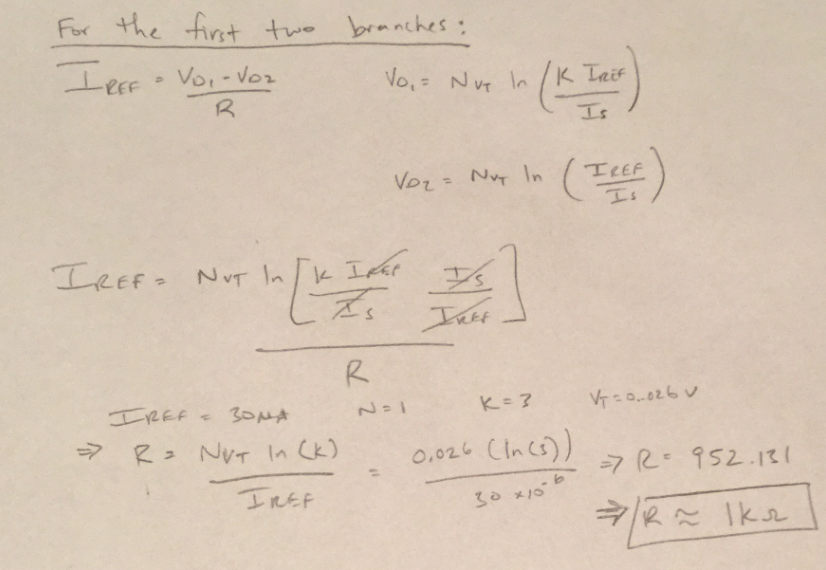
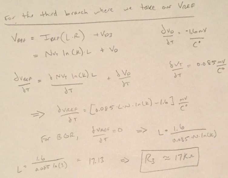
In order to build a BGR, we combined a CTAT (diode referenced self-biasing circuit), and PTAT (thermal voltage-referenced self-biasing) circuit. For CTAT, reference voltage goes down with an increase in temperature mainly because the diode has a greater influence and a diode's current increases with an increase in temperature. And for PTAT, reference voltage goes up with an increase in temperature. Because the circuit is a current mirror, the PTAT makes the voltage on D1 the same as the voltage on our Resistor R2. R2 sets the current in the current mirror. We chose a current of 30uA. The calculation for choosing the Resistor size is shown below. We chose a K of 3 for our diodes simply to minimize the number of components used, but the number of diodes are more than one because we need a voltage drop across the resistor in order for a current to flow. This current is then driven into the branch where we have the voltage reference. This branch is CTAT due to the higher Resistive load.
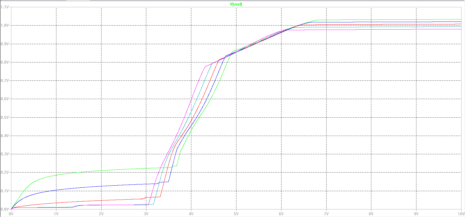
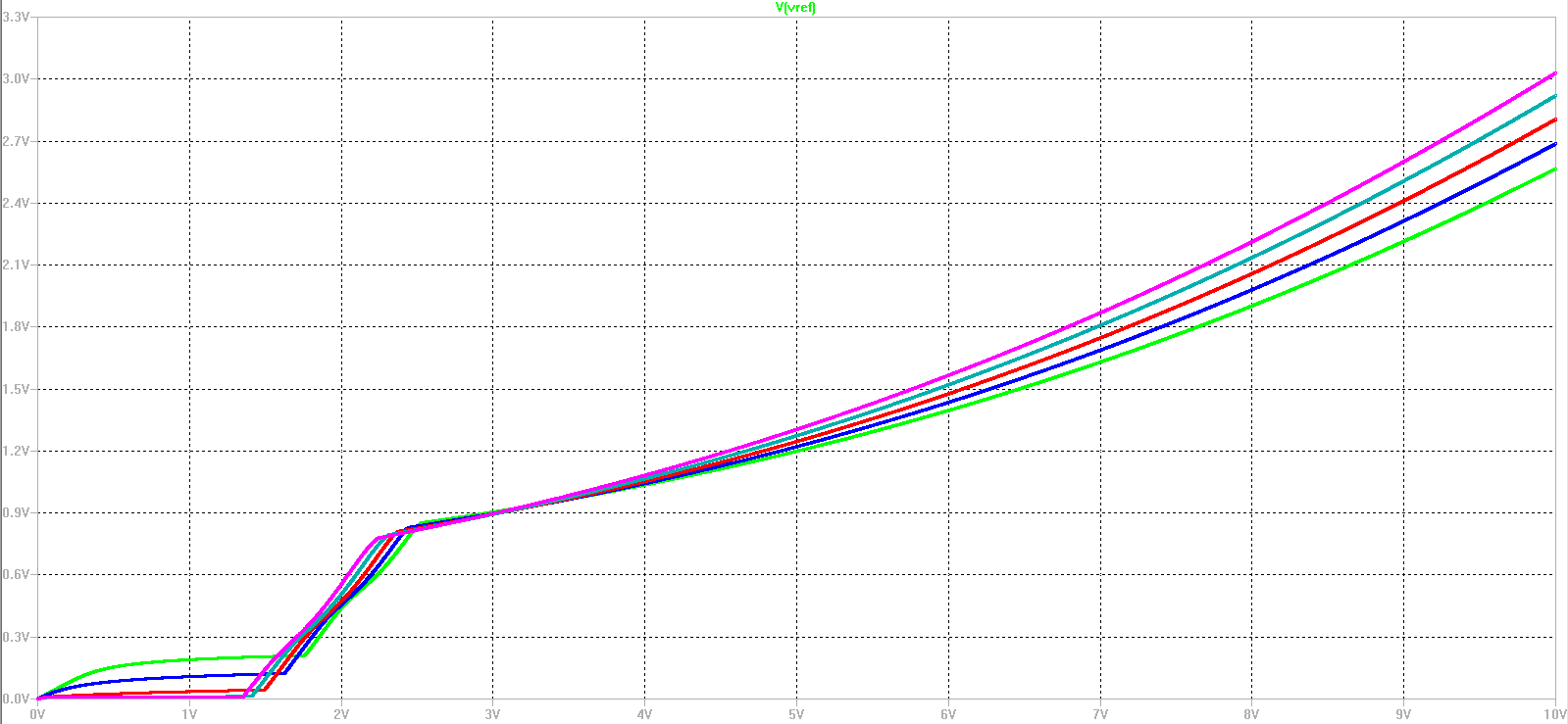 | Our simulation based on our device model shows that we don't have much variation with temperature with the design we chose. It also shows that the minimum VDD for our circuit to operate is 2V, which gives us a reference voltage of 900mV, which then slowly rises to about 3V when we are at a VDD of 10V |
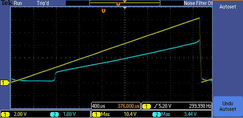 | The experimental results we obtained match our simulation plot almost exactly. The minimum VDD for our circuit to operate is 2V, which gives us a reference voltage of 900mV, which then slowly rises to about 3V. This means that the characterization of the transistors we previously did was spot on, and that variations in temperature, in theory, should give us the same results obtained fromt the simulation plots. Unfortunately we were unable to experimentally test for changes in temperature as a complete circuit. |
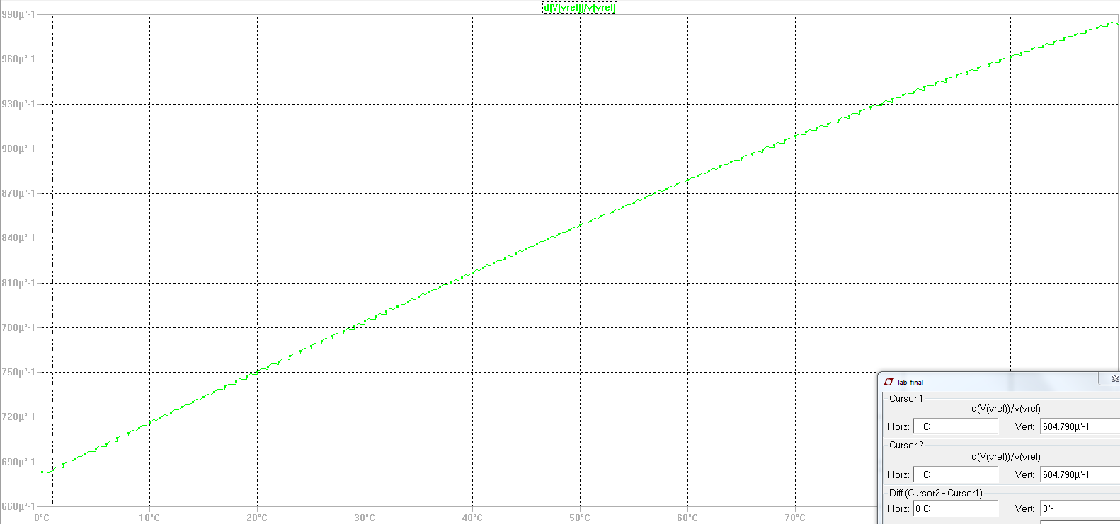 | This is the plot of the temperature coefficient of our Reference Voltage with a change in temperature. TC = (1/Vref)(dVref/dT) The plot indicates our TC at 765(microVolts/degreeCelcius) |
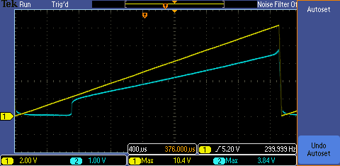 | These are the results when we increase the heat on the CTAT side of the circuit. We accomplished this by placing a heated up soldering iron directly on the leads of the K diodes. We notice that the on voltage for the circuit decreases along with voltage for a given VDD. |
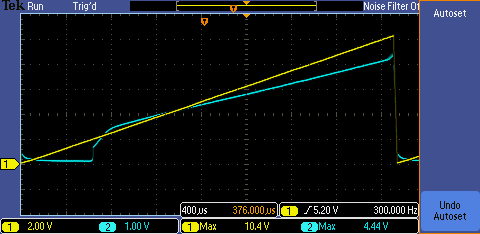 | These are the results when we increase the heater on teh PTAT side fo the circuit. We accomplished this by placing a heated up soldering iron directly on the leads of the K diodes. We noticed that the reference voltage increased for a given VDD. |
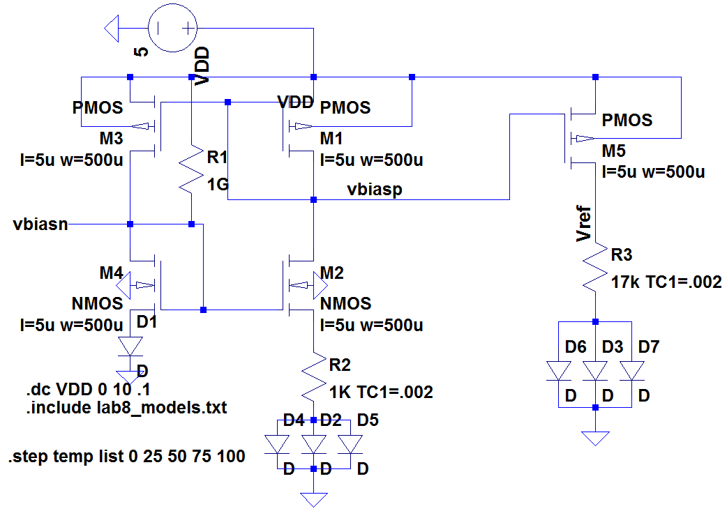
In conclusion, although we accomplished a circuit experimentally which was extremely similar to our simulations, but we were not able to have a constant voltage across a change in VDD. The way to solve this would be to apply a cascode structure to our circuit. Below is the schematic and simulation for such a design
|
|