Lab 9 - EE 420L
Dwayne K. Thomas
kendaleman@gmail.com
4/24/2015
Design of a Beta-Multiplier Reference
In this lab you may need to use two,
or more, CD4007 chips from the same production lot (see date code on
the top of chip) to ensure using a BMR to bias a current mirror is
possible. If the CD4007 chips are not from the same production lot they
will not "match" so current mirrors will not be possible.
- Build your BMR design and characterize it as you did in the pre-lab
- You
expect the BMR to become unstable if there is a large capacitance
across the resistor, such as a scope probe (important), so care must be
exercised
- Use your BMR to bias, and thus create, a:
- NMOS current mirror
- PMOS current mirror
- Measure how the current varies through each current mirror as the voltage across the mirror changes.
- Of
course the current in the NMOS (PMOS) current mirror goes to zero as
the voltage on the drain of the output device moves towards ground (VDD)
- Using these current mirrors drive two gate-drain connected transistors
- For the first experiment use the NMOS current mirror to drive two PMOS gate-drain connected devices.
- Use
the voltages on the gate-drain connection of the two devices to bias a
cascode current mirror (characterize this mirror as before)
- For the second experiment switch, that is, use the PMOS current mirror to drive two NMOS gate-drain connected devices.
- Again, use these two voltages to bias an NMOS cascode current mirror then characterize.
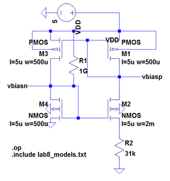
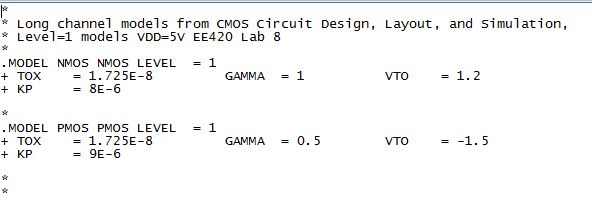
Using the PMOS and NMOS models created from the
measured information in the previous lab, we calculated a K value for
our BMR that allows us to have a constant gm of 20uA/V. The
calculation for this is shown below.
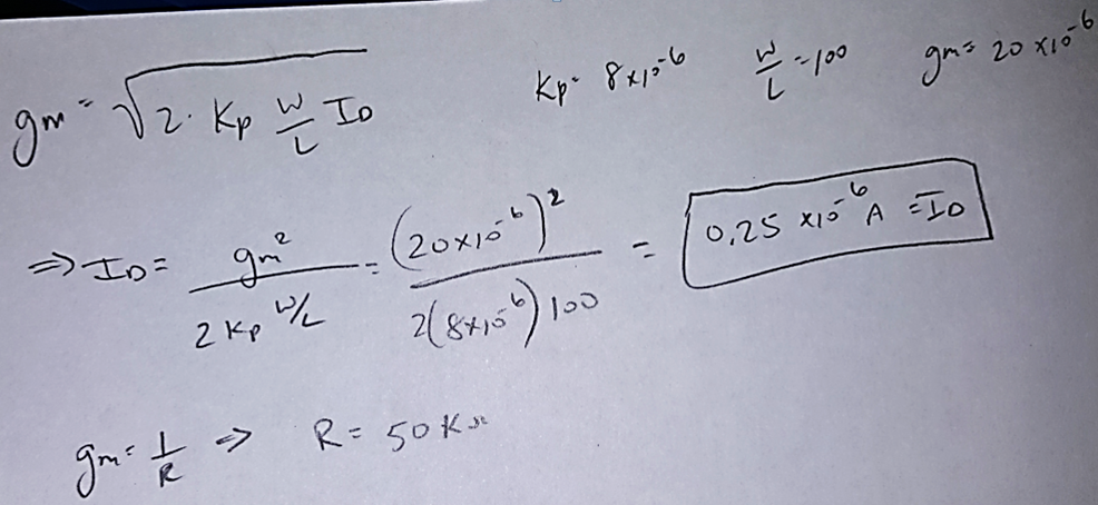
We calculated the Resistance at 50kohm in order to accomplish a gm of 20uA/V and a K of 4.
We used a 31kohm instead of the 50kohm resistor in order to obtain the values we need from our created Spice model
Experiment Results
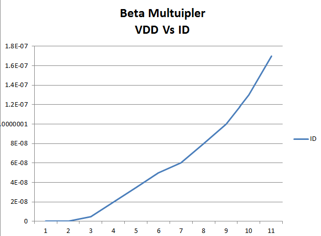
| This plot shows the VDD vs ID of the beta multilier as we sweep VDD from 0 to 10V |
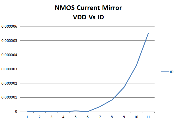
| The plot to the left shows the VDD vs ID for the NMOS current mirror |
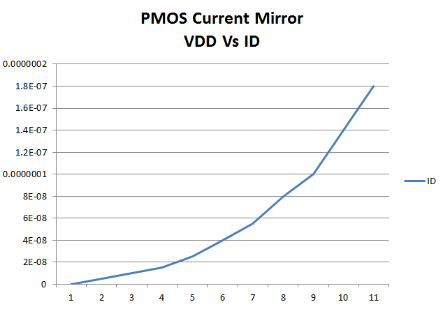
| To the left is a depiction of VDD vs ID for the current through the PMOS current mirror |
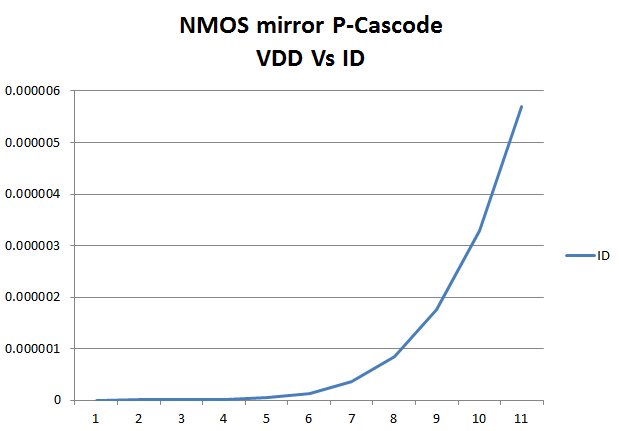 | To the left is the plot of VDD vs ID when we used the NMOS current mirror to drive two gate-drain connected PMOS transistors |
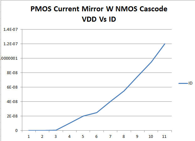 | To the left is the plot of VDD vs ID when we used the PMOS current mirror to drive two Gate-Drain connected N-MOS transistors |
Conclusion:
Building a BMR is not an easy task. Many issues can arise, such
as oscillation due to an incorrect Resistor size, Incorrect
wiring connections or bad chips. Care must be taken in order to
use chips that were made on the same day. This would help us more
with the matching problems we have to deal with.
Return to EE420 labs