Lab 8 - EE 420L
Dwayne K. Thomas
kendaleman@gmail.com
4/17/2015
Characterization of the CD4007 Transistor Array
- Experimentally generate, for the NMOS device, plots of:
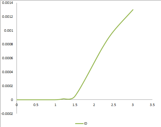
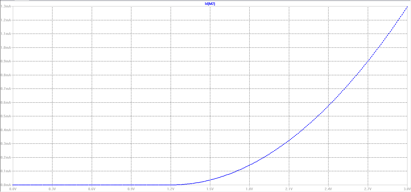
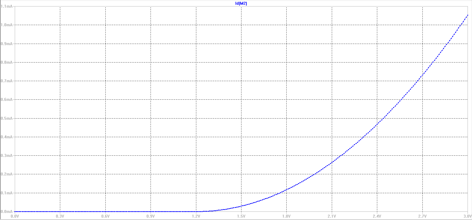
- ID v. VGS (0 < VGS < 3 V) with VDS = 3 V
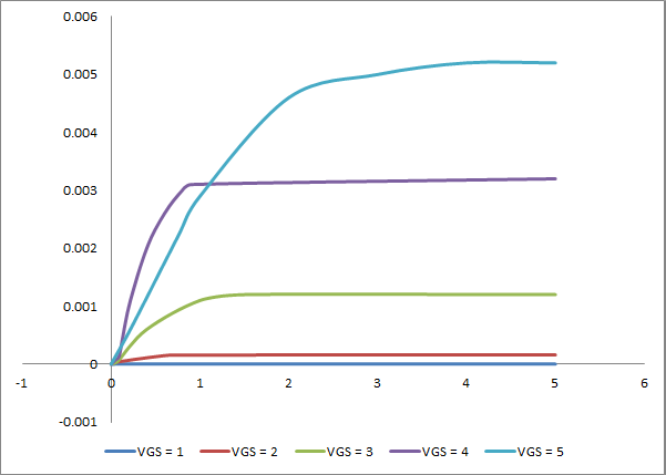
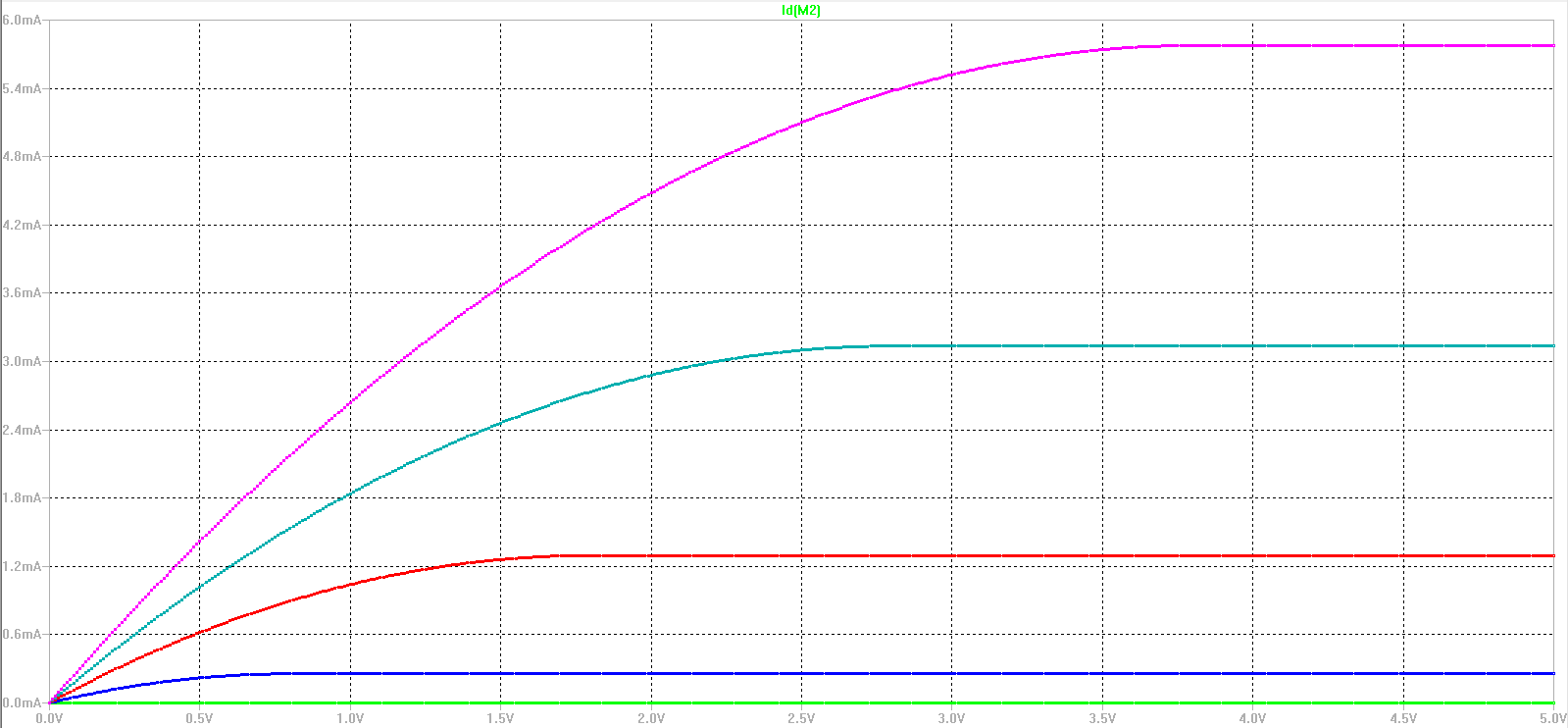
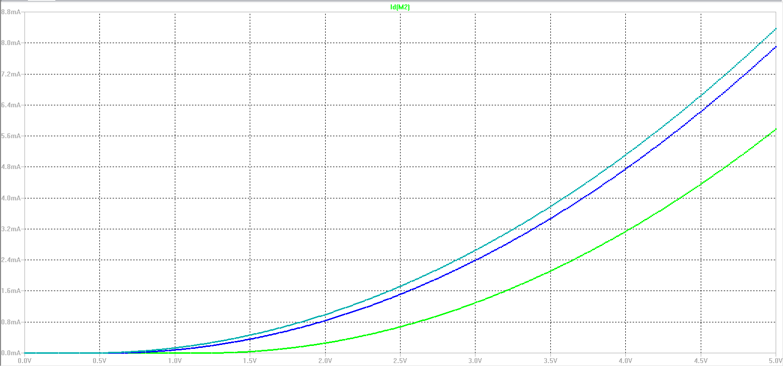
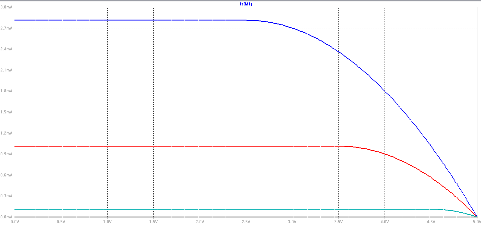
- ID v. VDS (0 < VDS < 5 V) for VGS varying from 1 to 5 V in 1 V steps, and
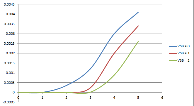
- ID v. VGS (0 < VGS < 5 V) with VDS = 5 V for VSB varying from 0 to 3 V in 1 V steps.
VGS vs ID for the NMOS transistor on the left along with the SPICE model simulation using calculated and adjusted parameters on the right
 |  |
| VDS vs ID for NMOS with step changes in VGS | Spice simulation for VDS vs ID |
|  |
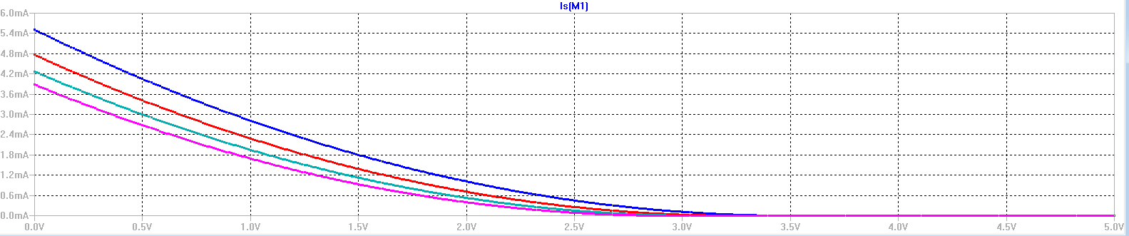
| VGS vs ID for changes in VBS | VGS vs ID for changes in VBS Spice simulation |
 |  |
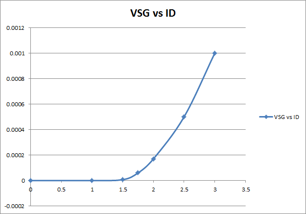
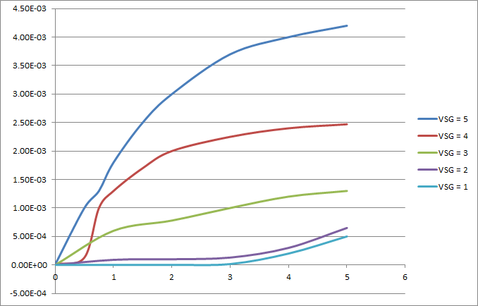
VSG
vs ID for the PMOS transistor on the left along with the SPICE model
simulation using calculated and adjusted parameters on the right
| 
|
| VSD vs ID for the PMOS | Simulaition for VSD vs ID for PMOS |
 | 
|
 Due
to limitations in the measuring equipment of teh TBE350lab and
operation hours of the lab, we could not obtain measurements for the
body effect of the PMOS transistor. Therefore the gamma for teh PMOS in
the calculations is an approximation based off teh SPICE simulation
from my input paramters. Due
to limitations in the measuring equipment of teh TBE350lab and
operation hours of the lab, we could not obtain measurements for the
body effect of the PMOS transistor. Therefore the gamma for teh PMOS in
the calculations is an approximation based off teh SPICE simulation
from my input paramters. |
The calculations for my paramters are as follows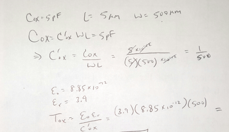
Kp = (2 x ID)/(VDSsat^2 x W/L)
Gamma = d(VTH)/d(VBS)
Using the Calculations above and our collected data: I obtained the following paramters:
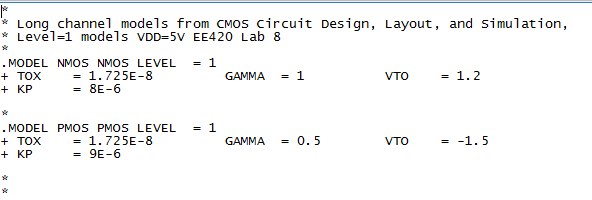
Vtop = 1.5V Vton = 1.2V Tox = 1.76 x 10^-8
Kpp = 10 Kpn = 14.8
Gamma for Pmos is approximately 0.5
Gamma for Nmos is apporxiamtel 1Below is the adjusted SPICE model initially created with the above parameters but then adjusted to match plots
Measurement of the Inverter rise/fall time is below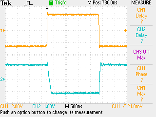
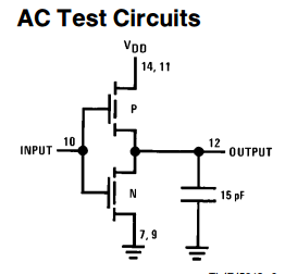
The inverter circuit was provided by the datasheet of the chip
and it was measured to be approimately 20 nanoseconds
Return to EE420 labs