Lab 6 - EE420L
Dwayne K. Thomas
kendaleman@gmail.com
3/20/2015
Single-stage transistor amplifiers
Experiment 1: The common-drain amplifier
These are the simulation results of the amplifier | 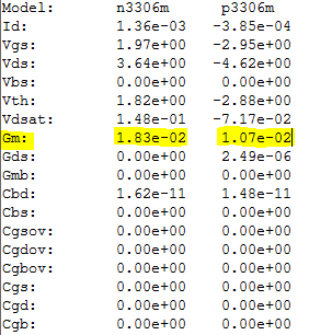 |
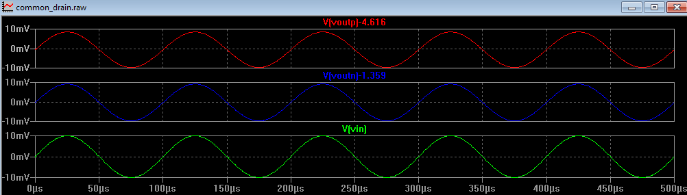 |
The common-drain amplifier is also
known as the source follower amplifier. It is called common-drain because
both the input and the output have the drain in common. It is called a source follower because the output of the
amplifier is located at the source and follows the signal at the input.
This amplifier configuration has a voltage gain close 1 which is
calculated further below.
| Amplifier circuits | NMOS circuit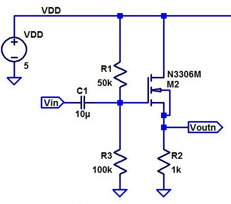 | PMOS circuit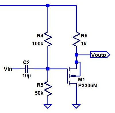 |
| Scope reading of the gain | 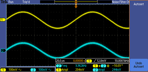 | |
| Scope reading of the Input Resistance Test |  | 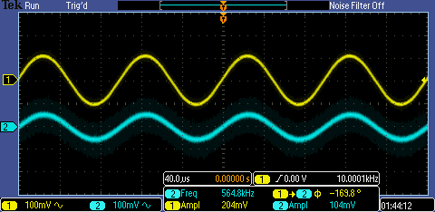 |
| Scope reading of the Output Resistance Test | 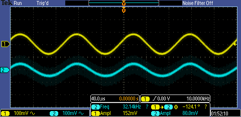 | 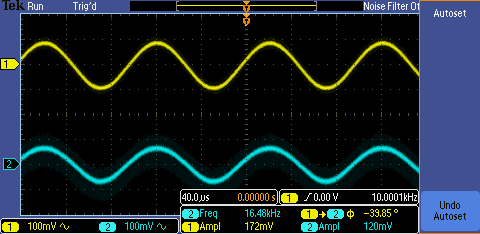 |
| In
order to test the input and output resistance of the circuit, we
connect a resistor in series that is the size of our caculated
resistance and apply a test voltage. If our calculated resistance
is correct, the resistor we place in series will have a voltage drop of
half of our test voltage. If not, the equation on right helps us
calculate the measured Resistance. | 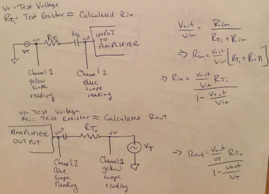 |
Below
are the calculations for INput Resistance, OUTput Resistance and gain
of the amplifier. We will use 18mV for the gm of the NMOS and
11mV for the gm of the PMOS. These are the values which also
obtained in the .op simulation of our circuit. Although they are
not exact due to the changing of gm. They will help us stay
consistent with our calculations throughout our experiments.
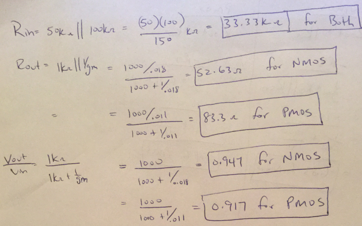
| Common-Drain amplifier Table | Calculated Gain | Measured Gain | Calculated input Resistance | Measured Input Resistance | Calculated Output Resistance | Measured Output Resistance |
| NMOS amplifier | 0.947 | 1.2 | 33.33k ohm | 26.4k ohms | 52.63 ohms | 58.5 ohms |
| PMOS amplifier | 0.947 | 1.2 | 33.33k ohm | 34.7k ohms | 83.3 ohms | 192 ohms |
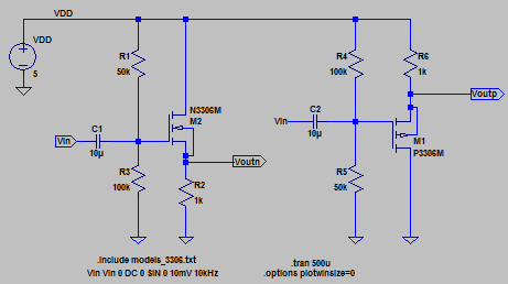
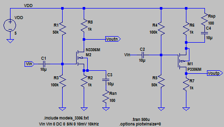
Experiment 2: The common-source amplifier
 To the left is our simulation schematic and below are out simulation results To the left is our simulation schematic and below are out simulation results |
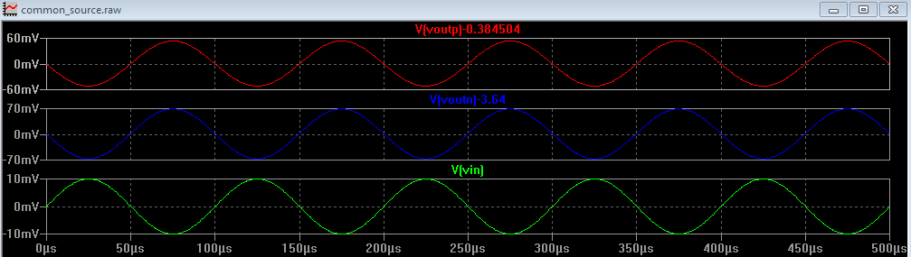 |
The
common-source amplifier is called common-source because
both the input and the output have the source in common. R1 and
R3 create a voltage divider to bias the gate voltage on the NMOS.
This is also accomplished by R4 and R5 in the PMOS circuit.
The input is capacitively coupled on both circuits to maintain
the biasing.
| Amplifier circuits | NMOS circuit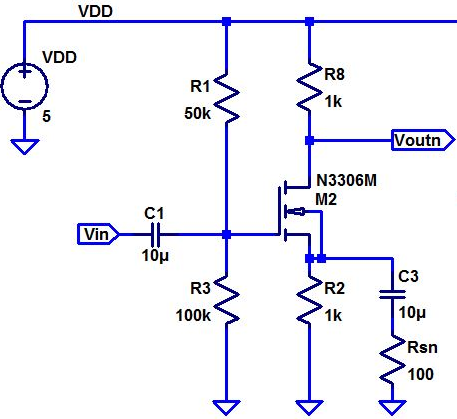 | PMOS circuit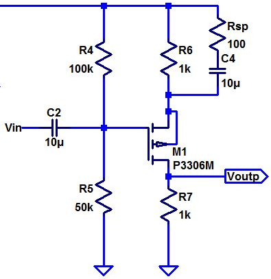 |
| Scope reading of the gain | 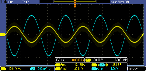 | 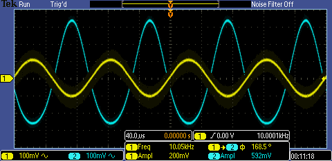 |
| Scope reading of the Input Resistance Test | | |
| Scope reading of the Output Resistance Test | 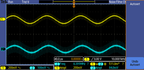 | 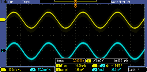 |
Below
are the calculations for
INput Resistance, OUTput Resistance and gain of the amplifier. We
will
use 18mV for the gm of the NMOS and 11mV for the gm of the PMOS.
We notice that increasing the Rsn or Rsp, decreases our gain.
| Common-source amplifier Table | Calculated Gain | Measured Gain | Calculated input Resistance | Measured Input Resistance | Calculated Output Resistance | Measured Output Resistance |
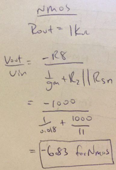
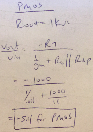
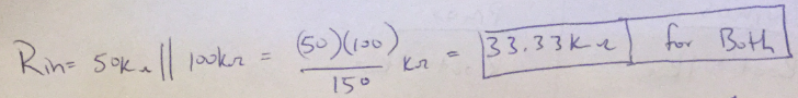
| NMOS amplifier | -6.83 | -5.2 | 33.33k ohm | 26.4k ohm | 1k ohm | 724 ohm |
| PMOS amplifier | -5.4 | -2.96 | 33.33k ohm | 34.7k ohm | 1k ohm | 960 ohm |
The large difference in gain of our PMOS can be due to gm that is very different from what we used to caculate
Experiment 3: The common-gate amplifier
 These are the simulation results of the amplifier These are the simulation results of the amplifier |
 |
| Amplifier circuits | NMOS circuit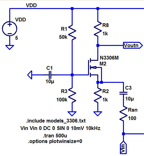 | PMOS circuit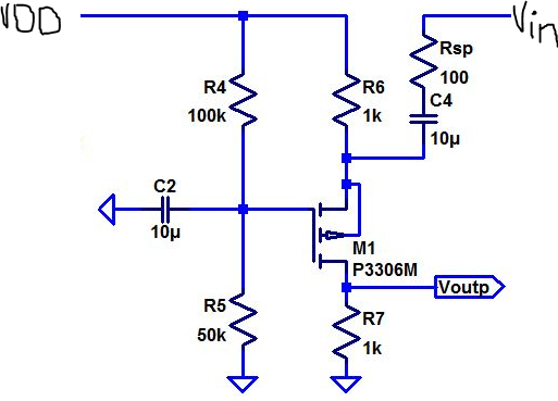 |
| Scope reading of the gain | 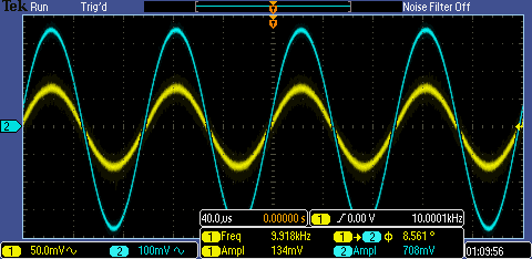 | 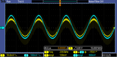 |
| Scope reading of the Input Resistance Test |
|  |  |
| Scope reading of the Output Resistance Test |  | 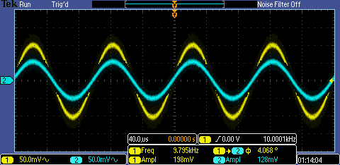 |
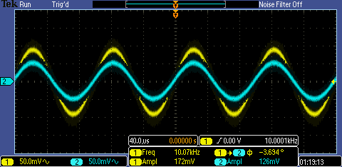
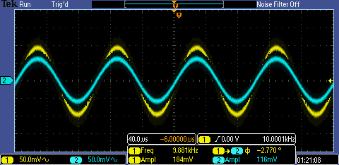
Below are the calculations for
INput Resistance, OUTput Resistance and gain of the amplifier. We will
use 18mV for the gm of the NMOS and 11mV for the gm of the PMOS. We notice that increasing the Rsn or Rsp, decreases our gain.
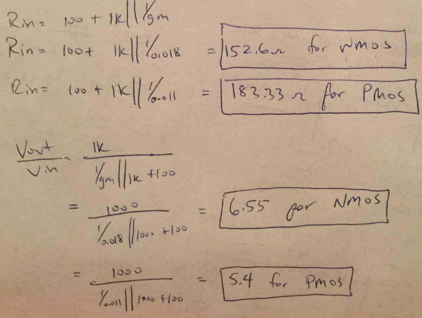
| Common-gate amplifier Table | Calculated Gain | Measured Gain | Calculated input Resistance | Measured Input Resistance | Calculated Output Resistance | Measured Output Resistance |
| NMOS amplifier | 6.55 | 5.28 | 152.6 ohm | 418 ohm | 1k ohm | 980 ohm |
| PMOS amplifier | 5.4 | 2.83 | 183.3 ohm | 335 ohm | 1k ohm | 1.8k ohm |
The large difference in gain of our PMOS can be due to gm that is very different from what we used to caculate
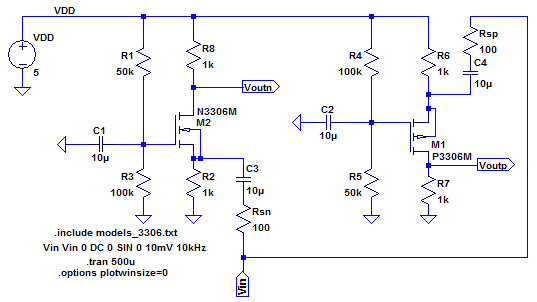
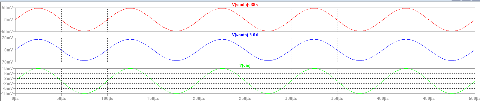
Experiment 4: The push-pull amplifier
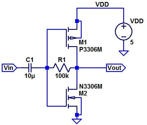
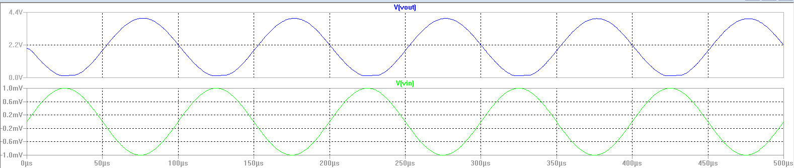
Above shows the PSPICE simulation results of the push-pull amplifier. The push pull
amplifier allows the sourcing and sinking of current. The resistor
allows for a constant DC voltage across the gate and sources of the
transistors. No current flows through the resistor, it is used as a
gain multiplier. Therefore as we increase the resistance from 100kohm
to 510kohm, we esentially multiply the original gain by 5.
| Hand Calculations | id = vsg1 * (gm1) id = vgs2 * (gm2)
because vsg = vgs = vin
Vout/Vin = (R1)*(gm1 +gm2)
Vout/Vin = 100k * (.011 + .018)
Vout/Vin = 2900 |
| Using a 100kohm Resistor | Using a 510kohm Resistor |
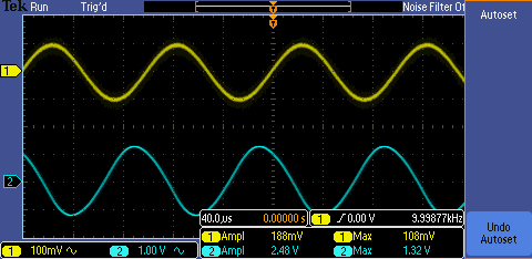 | 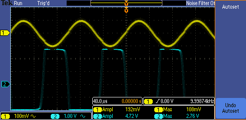 |
Return to EE420 labs