Lab 3 - EE 420L
Common Mode Voltage is the sum of Vp and Vm divided by
2.
Therefore the Maximum Common Mode Voltage would ideally be
(5 + 5) ÷ 2 = 5V
And our minimum Common Mode Voltage would be (0 + 0) ÷ 2 = 0V
But according to the datasheet for the Opamp, the maximum common mode voltage would be, VCC - 1.5V at ambient temperature.
So for our +VCC and –VCC chosen, the maximum would be 5V - 1.5 = 3.5V
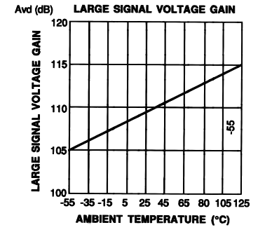
According to the datasheet for the Opamp, the large signal Voltage Gain is 100V/mV which is 100,000.

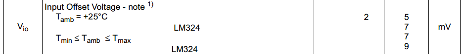
The datasheet shows offset voltage varying with temperature,
but normally sitting at 2mV. For worst
case design, I would use the max offset voltage of 9mv.
We built the circuit below for Experiment 1
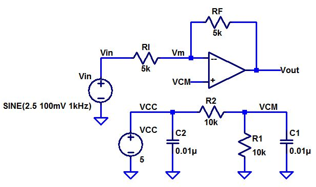
Our common-mode voltage is 2.5V
It does not change for our circuit because it is the DC value
we placed at VCM using a voltage divider.
In addition, the goal of the Opamp is to maintain the Vm and
Vp voltages at the same value.
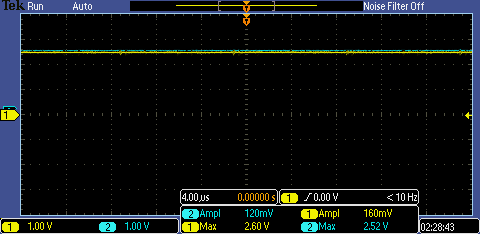
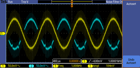
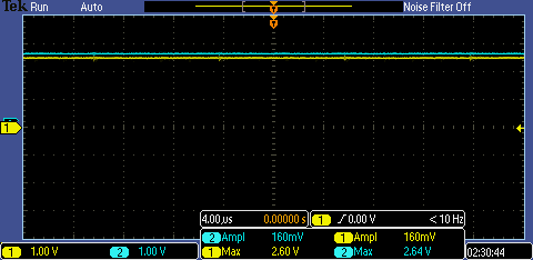
The output swing is 200mv centered around 2.5V
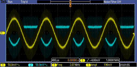
If the input isn’t centered around VCM, the output swing would still be 200mv, it would instead swing around a different DC value inverted from the input. This is because the direction of current will always be from the positive input going toward the negative output in this circuit. Since both our feedback and input resistors are the same value, the voltage drop across each resistor will be the same. Therefore as the DC voltage at the input is increased positively, the DC voltage at the output increases negatively, or in other words goes down. But the AC voltage will remain the same amplitude.
The Maximum allowable input signal amplitude is 1.25V, because
if we increase the amplitude higher than this, our output will begin to clip in
its negative cycle which coincides with positive cycle of our input. This is due to our limited Maximum Common
mode voltage of 3.5V.
The purpose of the capacitors from VCC and VCM to ground is to act as AC short to ground. We only want a constant DC voltage at our VCM, therefore these capacitors short out any noise and higher frequencies that might be coming from our source.
Input offset current is the difference between the current flowing into and out of the Vplus and Vminus inputs of the Opamp which are the respective bias currents. This offset in current causes the difference in voltage at the Vp and Vm to increase as larger resistors are used. This is due to the larger voltage across the larger resistors which make this current difference mor visible.
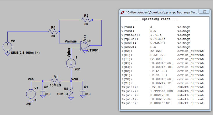
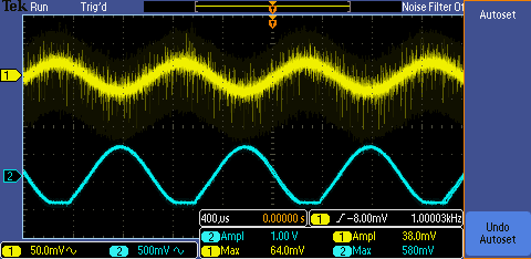
This current can drastically affect the output of the
circuit. When we built the circuit, we measured
our output to swing around 900mv with the same AC amplitude of 100mv. And Vcm and Vm had a difference of
900mv. We simulated the circuit in spice simulation above
by using a current source to simulate 20nA of offset current, and the spice
simulation verified our real life results.
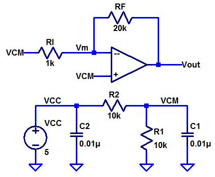
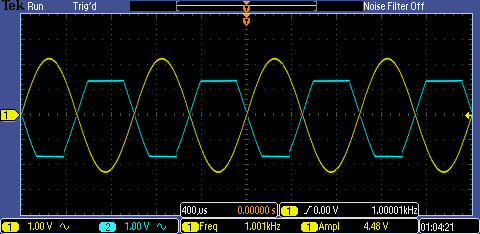
The above circuit can be used to measure the offset
voltage by placing this offset across the input resistor. This voltage can then be amplified by the
output by a factor of 20 so that it is more noticeable due to Vout = (Rf/Ri)(Vcm-Vm) therefore
(Vout – Vm)/20 = Vcm -Vm ,
since Vcm – Vm = Voffset , then
Voffset = (Vout – Vm)/20
 After measuring 4 different opamps, we found that three of
them had an offset voltage of 2mV as per the datasheet. But one of them had an offset voltage of
4mV. This shows us that not all Opamps
of the same model will the exact same test results. In real life situations, they can be slightly
different.
After measuring 4 different opamps, we found that three of
them had an offset voltage of 2mV as per the datasheet. But one of them had an offset voltage of
4mV. This shows us that not all Opamps
of the same model will the exact same test results. In real life situations, they can be slightly
different.