
Lab 9 - ECE 420L
Build your BMR design and characterize it as you did in the pre-lab. You expect the BMR to become unstable if there is a large capacitance across the resistor, such as a scope probe (important), so care must be exercised.
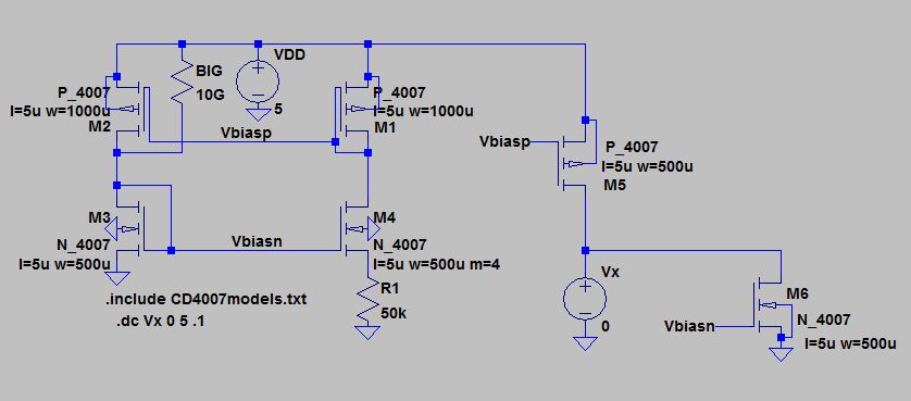
From the prelab, the BMR that was designed in LTspice is shown below. The 10 Giga Ohm resistor is there to "leak" in current so that the transistors start up in their proper state instead of the unwanted state in which there is not current flowing at all. From lab 8, the KPn is almost double the value of the KPp. So, in order to properly create a current mirror, the widths of the PMOS are double than that of the NMOS. According to lab 8, I will assume that the length of both PMOS and NMOS is 5 um and the width is 500 um. Therefore, the PMOS will have a width of 1000 um. For the BMR, the k (m in the schematic) is chosen to be 4 in order to obtain the so-called "constant-gm bias circuit" in which R = 1/gm. Since the gm is supposed to be 20 uA/V, the R should be about 50k.
The simulation result is shown below.

The actual implementation on a breadboard involved putting two PMOS in parallel in order to obtain a width of 1000 um, that is of course assuming the assumption of a width of 500 um for a single PMOS/NMOS transistor is valid. This means that the m = 4 was implemented by putting 4 PMOS in parallel. The start up resistor was made out of three 20 mega-Ohm resistors in series because we did not have any 10 giga-Ohm resistors lying around in lab. After an hour and a half or so of tedius wiring, the circuit shown below was made.

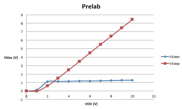
Then, the VDD was swept and the Vbiasn and Vbiasp were measured and recorded on an Excel document. Then, they were ploted on the same graph with VDD on the X-axis and Vbiasn/Vbiasp on the Y-axis. The resulting graph is shown below.
When a 1000 uF capacitor shunts the 50k resistor and VDD is a 1 volt square pulse, the following instability is shown for Vbiasn and Vbiasp. I could not plot the current using the oscilloscopes in lab.

Use your BMR to
bias, and thus create, a:
NMOS current mirror
The schematic for the basic NMOS and PMOS current mirrors are shown below.
Measure how the
current varies through each current mirror as the voltage across the
mirror changes.
Of course the current in the NMOS (PMOS) current mirror goes to zero as the voltage on the drain of the output device moves towards ground (VDD).
The simulation results for the basic NMOS/PMOS mirrors are shown below. ID(M6) corresponds to the NMOS and ID(M5) corresponds to the PMOS.

The results for the actual lab implementation were obtained by varying the voltage source called Vx in the schematic from 0 to 5 Volts. The NMOS current mirror was done seperately from the PMOS current mirror. For some reason, all the multimeters in the 350 lab have their fuses blown out, so I could not measure current directly. So, I had to put a 1k resistor in series with the Vx voltage source and measure the potential difference across the resistor. The rest is just basic Ohm's law to determine the current flowing in the resistor, which should be the same as in the current mirror, at least in theory anyway. Again, each current mirror was tested seperately in lab, which is different in the schematic which shows them being simulated at the same time. Also, the LTspice schematic does not show the series 1k resistor. The data was recorded on Excel and then the data was ploted with Vx in the X-axis and ID in the Y-axis. The graphs of the lab results are shown below.
| NMOS current mirror | PMOS current mirror |
 |  |
In the Excel plots shown above, the voltage for Vx only goes up to 1.2 volts because the curent stayed at a nominal value of 11.5 uAfor all voltages between 1.2 and 5 volts. In other words, it stayed constant after 1.2 volts. The plot for the PMOS current mirror should stay at a constant current after awhile, but the volmeter in lab would not give very steady readings, so the current seems to increase when it probably stayed constant value between 4 and 5 uA.
Using these current mirrors drive two gate-drain connected transistors
For the first experiment use the NMOS current mirror to drive two PMOS gate-drain connected devices.
Use the voltages on the gate-drain connection of the two devices to bias a cascode current mirror (characterize this mirror as before)
The lab directions are essentially saying "build a cascode current source." Using the NMOS current mirror previously built and the gate-drain connected PMOS transistors, the following schematic is built.

Vx is then swept from 0 to 5 volts, and the following current is sumulated for the right side branch.

In lab, the cascode was built and following the same procedure from the NMOS/PMOS current mirrors, the following data was recorded and plotted in Excel. For this cascode, I did not have enough CD4007 chips to build it with the double PMOS width. So, I did not double the PMOS width, but instead I doubled the length of the NMOS from 5 um to 10 um by putting two NMOS in series. This is so their gm are nearly equal.

For the second experiment switch, that is, use the PMOS current mirror to drive two NMOS gate-drain connected devices.
Again, use these two voltages to bias an NMOS cascode current mirror then characterize.
Again, this is asking us to build a cascode current source but with the twist that the NMOS and PMOS switch places. The schematic is shown below.

Vx is again varied and the simulation results are shown below.

The data obtained for lab was again recorded and ploted on Excel. This is shown below.

As with the NMOS current mirror, the value stayed at a constant value at a certain voltage, so the plot only goes up to 1.2 volts.
Below is the schematic for the entire circuit.

Below is the values for Vbiasn and Vbiasp that appeared for most of the experiments at VDD = 5V
| Vbiasn | Vbiasp |
 |  |
In conclusion, the simulation results and experimental results seem to match in terms of what the plot is supposed to look like. However, the values for current in the simulations are in the nano-amp range while the experimental results are in the micro-amp range. This is probably because the models in the simulations used are not very accurate. Also, the small current flowing in the transistors are probably affected by the resistance in the wires used to make the measurements. I would also like to thank professor Baker for taking time out of his busy schedule to make this extra lab assignment for us.
As always, I will backup my work as shwon below.
