EE 420L - Project
Design of a Bandgap Voltage References (BGR) using the CD4007 CMOS transistor array
Authored
by Nicholas Moya
April 30rd, 2015
moyan1@unlv.nevada.edu
The
purpose of this lab is to build a bandgap voltage reference circuit
using the CD4007 chip. In this report, we have my partner and I include design
considerations, simulation results and measured results showing the
BGR's performance including how the reference voltage changes with
VDD.
Theory of Operation
The
purpose of a bandgap reference (BGR) is to supply a constant voltage
reference that does not change with VDD nor changes in temperature.
This is accomplished by using current mirrors with resistors in series
with diodes withn their banches. This is the idea; the current flowing
through the current mirror branches is suppose to be the same, hence
the name. Because the current will be the same through both branches,
if we connect a resistor in one branch and a diode in the other, the
voltage drops must be the same (because the current is the same). This
gives us a relatively constant voltage drop with VDD.
However,
we want a voltage reference independent of VDD AND temperature, and a
resistor's voltage drop will increase with temperture. This
characteristic can be counteracted by the fact that the
voltage drop across a diode decreases with temperature. Therefore, we
must put a resistor in series with a diode on one branch along with a
diode on the other branch.
However,
we can not simply put the resistor in parallel with ONE diode as this
would cause the voltage on top of the resistor (~0.7) and the
voltage below the resistor (~0.7) to be the same, causing a voltage
drop of 0 and thus 0 current would flow. Thus, we must put k (in our
case 4) diodes in series with the resistor; this will cause a current
difference as the current splits to go through the different diodes
therefore making the voltage on top of the resistor larger than on the
bottom.
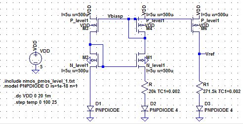
Lastly,
we connect a seperate PMOS branch from our Vbias1 node to provide a
Vref. Of course, we must include a resistor in series with k (4) diodes
in this new branch so it acts the same as our current mirror branches.
However, in this new branch, we can put a bigger resistor so as to
limit current, thus making Vref bigger. Putting all of this together,
gives us our schematic as provided below:
Design Calculations
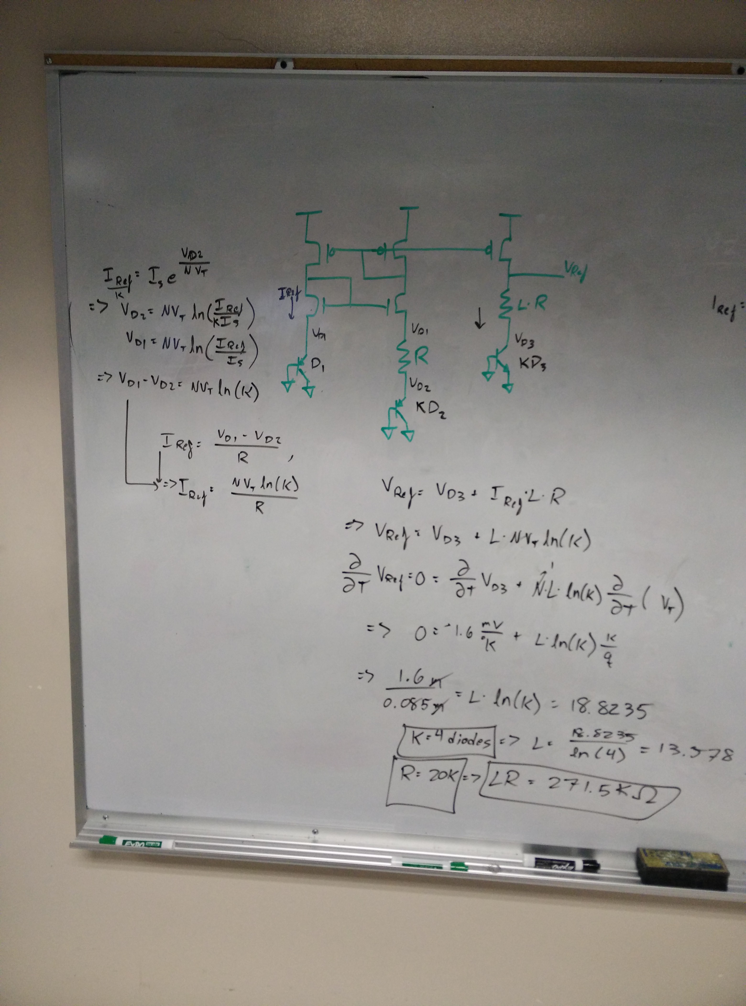
Temperaturen Coefficient calcuation
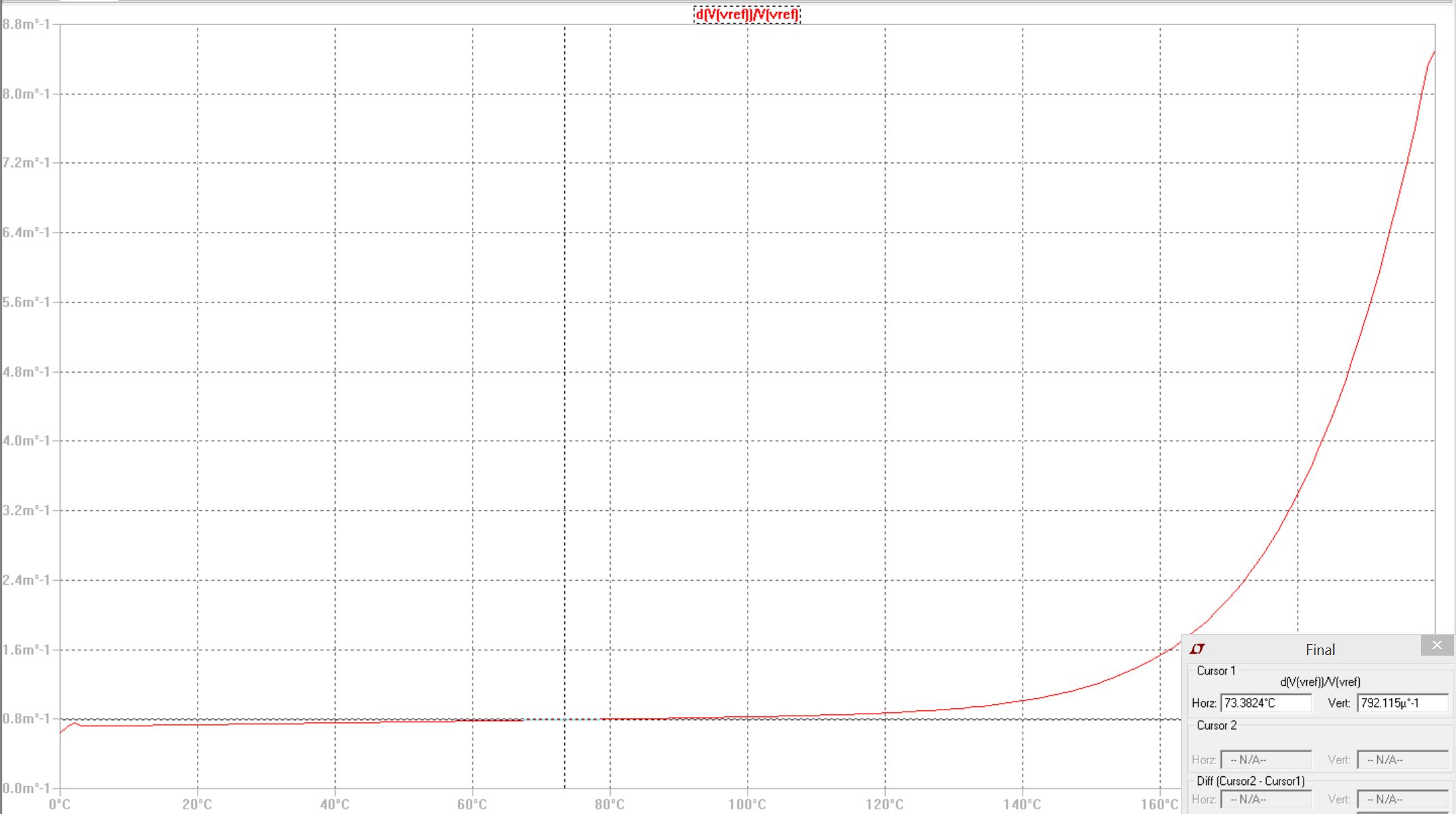
Simulated Results
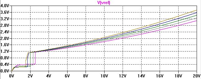
As
is evident from the simulation, our BGR is not completely invariant
with changes in VDD and temperature. Ideally, we want our voltage
reference, Vref, to stay at 1.2V as VDD increases from 2V and temperature change however
our simulation shows Vref goes from 1.2V to 3.2V for at 25 degrees
celsius. Similarly, Vref shows a max voltage difference of 0.56V
between 0 and 100 degrees celsius. While this result is a little better
we still calculate a overall change of roughly 5.6mV/C.
Measured Results
| VDD | Vbiasp | Vref |
| 0.998 | 0.03 | -0.0226 |
| 1.998 | 0.556 | 0.645 |
| 2.997 | 1.538 | 0.859 |
| 3.996 | 2.526 | 1.058 |
| 4.996 | 3.516 | 1.261 |
| 5.996 | 4.508 | 1.475 |
| 6.995 | 5.5 | 1.701 |
| 7.994 | 6.493 | 1.943 |
| 8.993 | 7.486 | 2.203 |
| 9.993 | 8.48 | 2.479 |
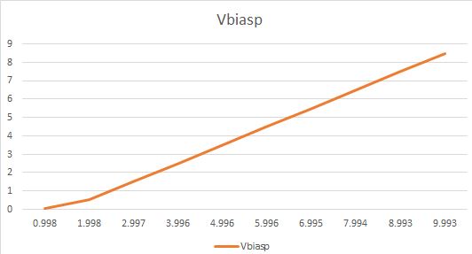
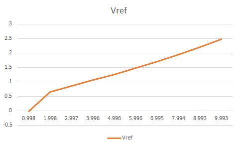
From
our measured results, we can see that our physical circuit fairs no
better as our Vref changes 1.8V from VDD = 2 to VDD = 10. This
discrepence can be attibuted to mismatching between the chips which
would cause the bias currents to be mismatched and thus effect our
Vref. A solution we could have employed would be to use a different
schematic such as the alternate topologies on page 767 of our CMOS book
in which op-amps are used to force the same current through each side
of our reference voltage.