EE 420L - Lab 8
Characterization of the CD4007 CMOS transistor array
Authored
by Nicholas Moya
April 16th, 2015
moyan1@unlv.nevada.edu
The purpose of this lab is to collect experimental data of the transistors used in the CD4007.pdf CMOS
transistor array, use that data to make parameters for simulations in
LTspice and compare the simulations with experimental data. After
comparison, we can augment our parameters to better simulate our
experimental results.
Experimentally generate, for the NMOS device, plots of:
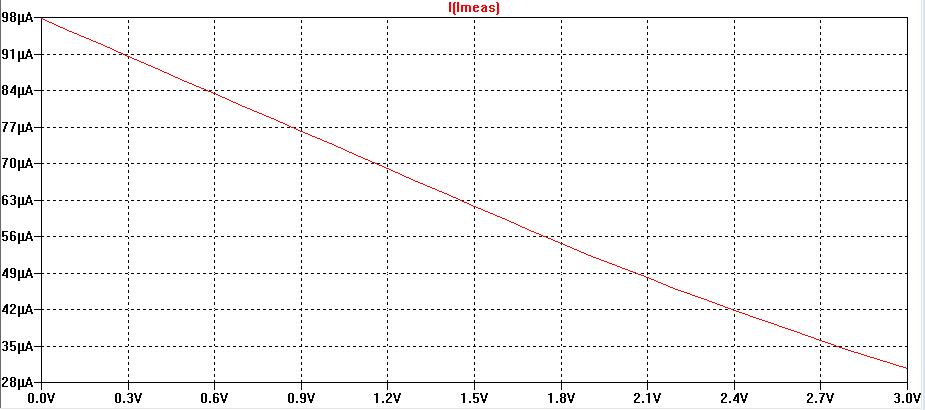
1. ID v. VGS (0 < VGS < 3 V) with VDS = 3 V
2. ID v. VDS (0 < VDS < 5 V) for VGS varying from 1 to 5 V in 1 V steps, and
3. ID v. VGS (0 < VGS < 5 V) with VDS = 5 V for VSB varying from 0 to 3 V in 1 V steps.
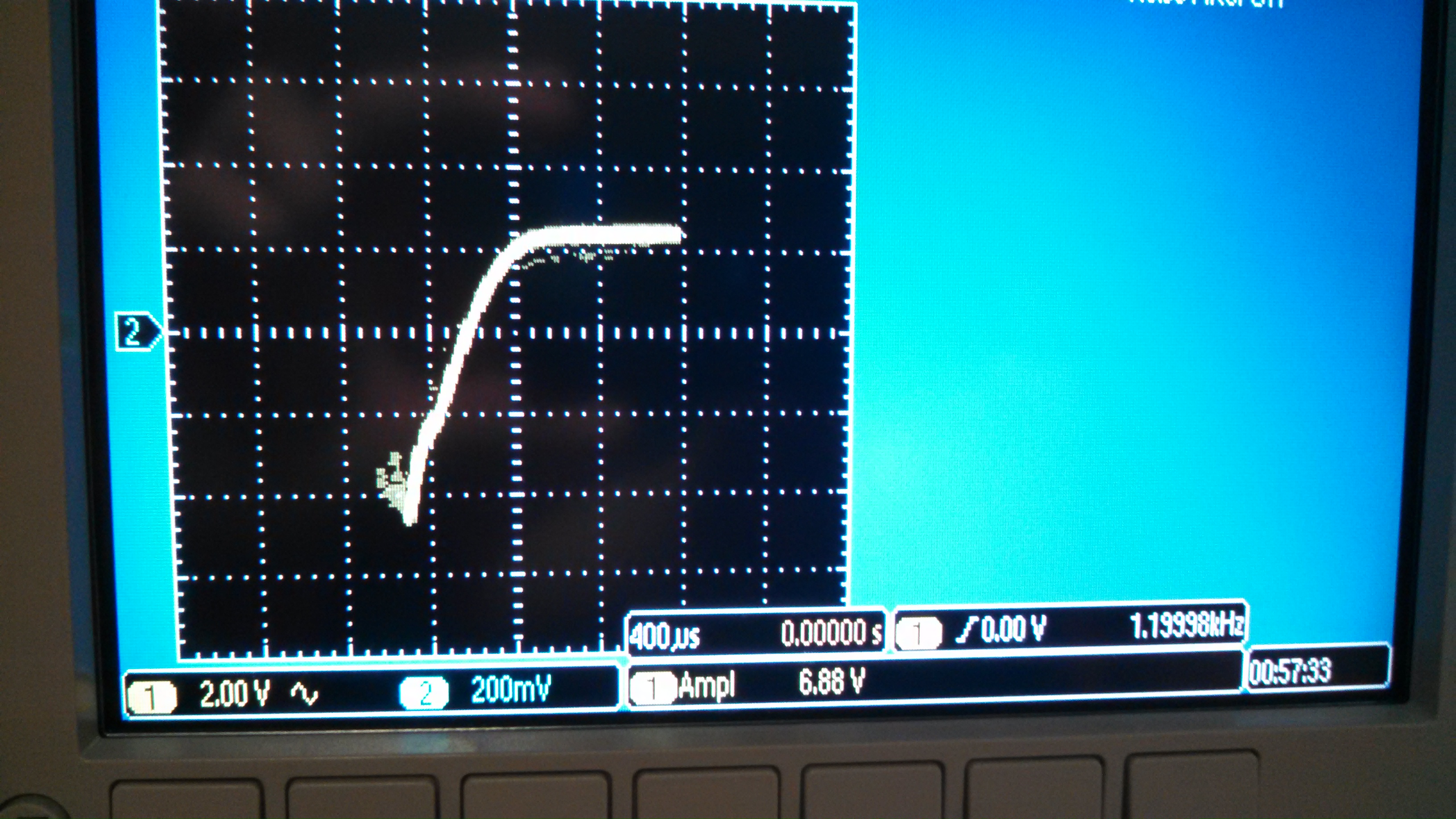
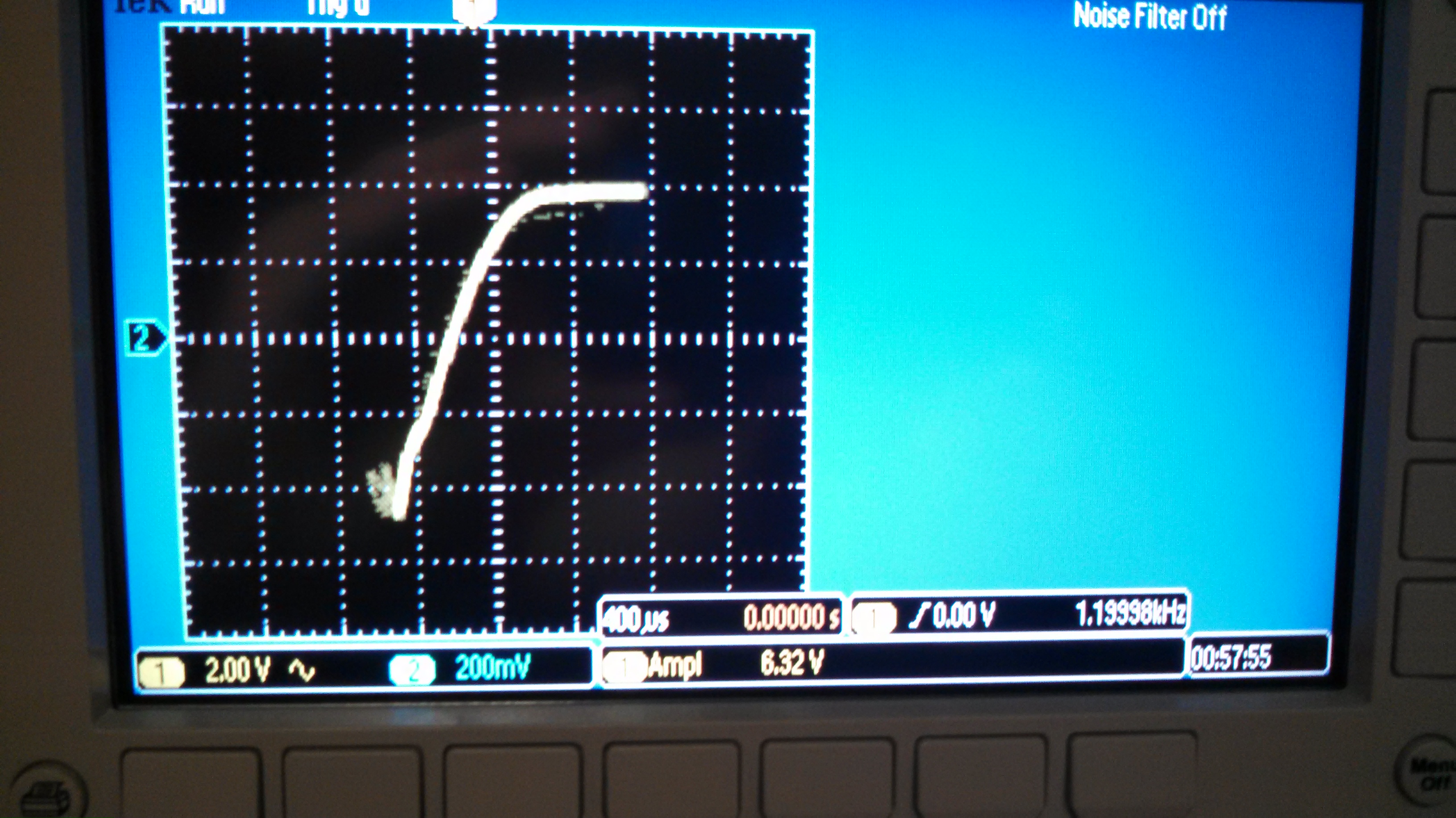
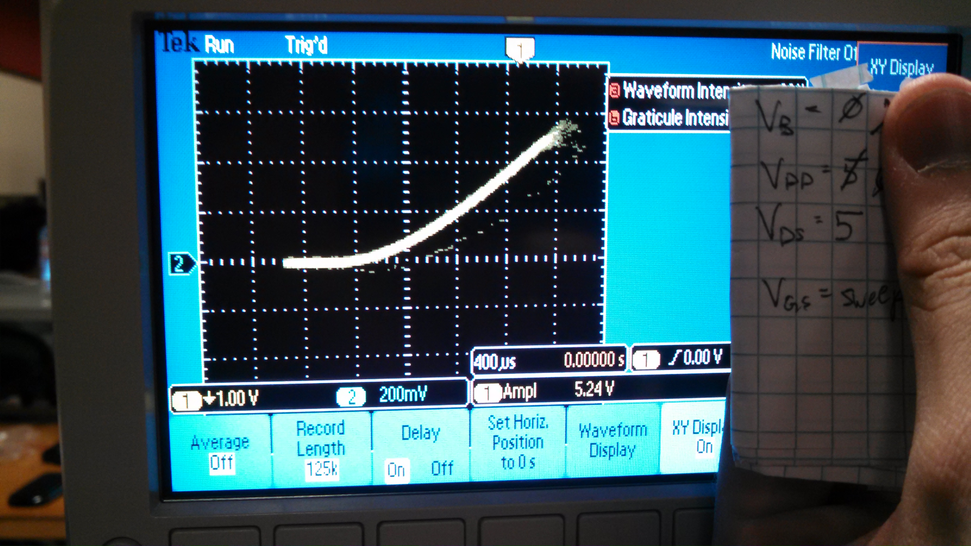
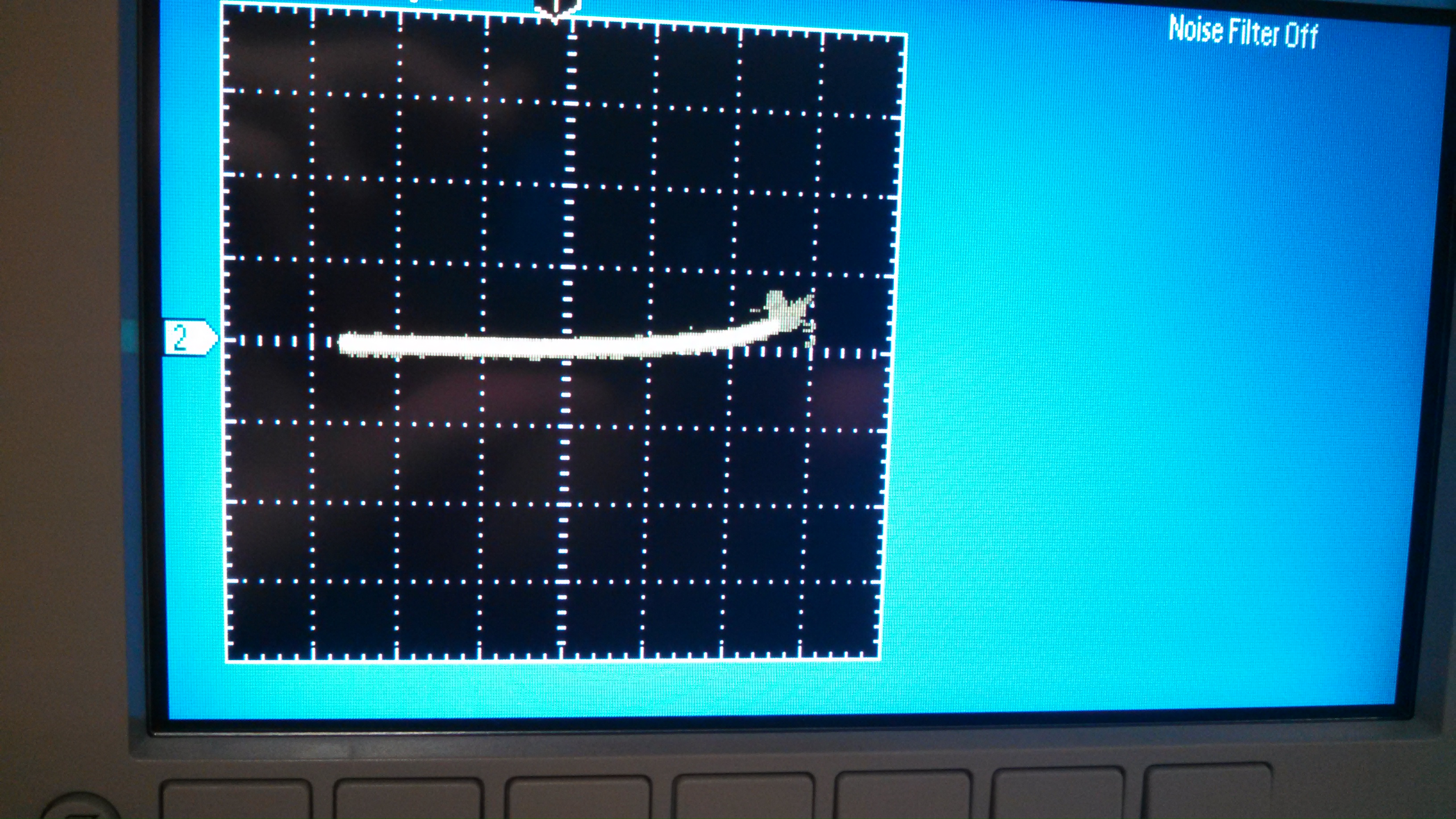
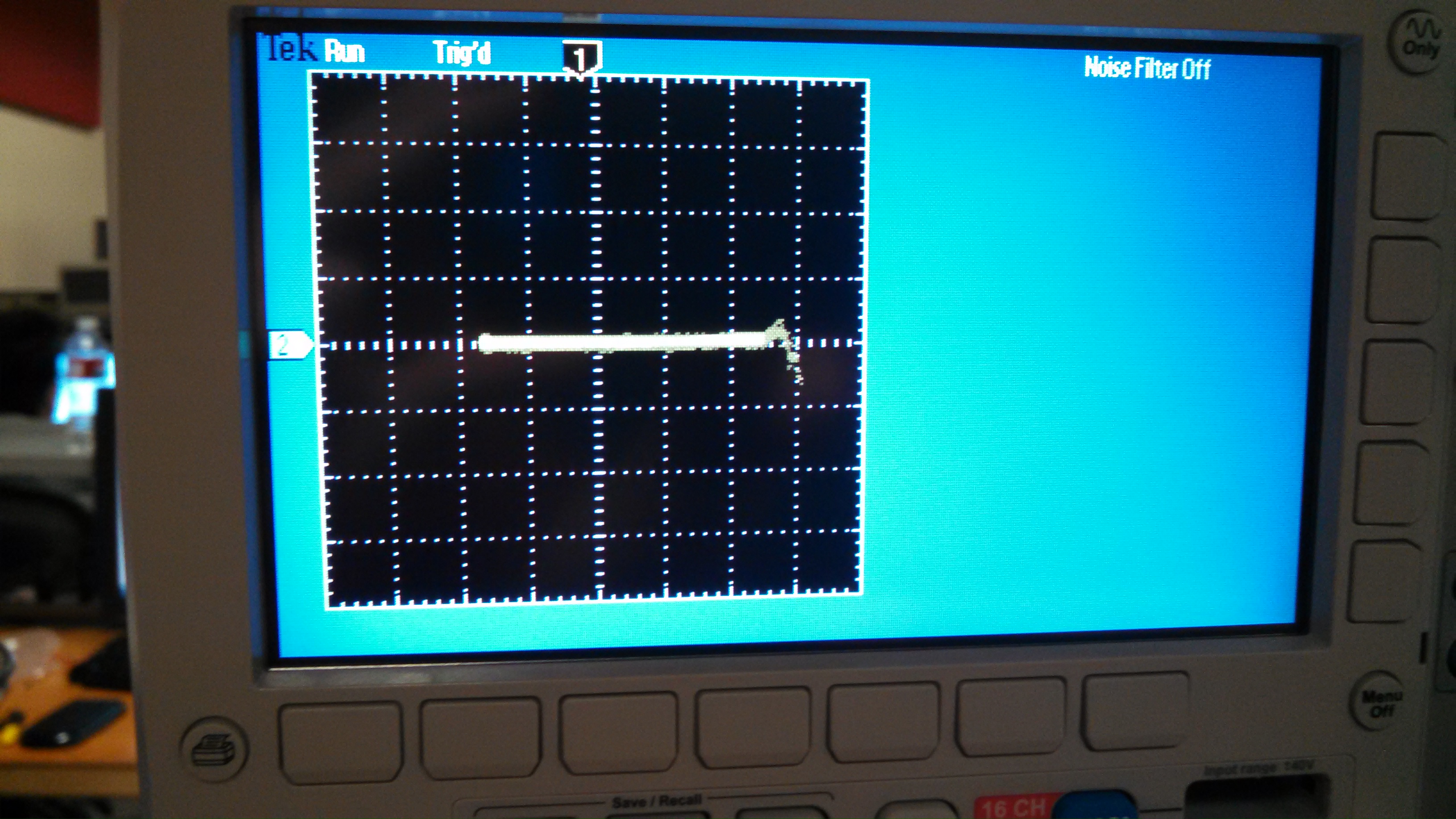
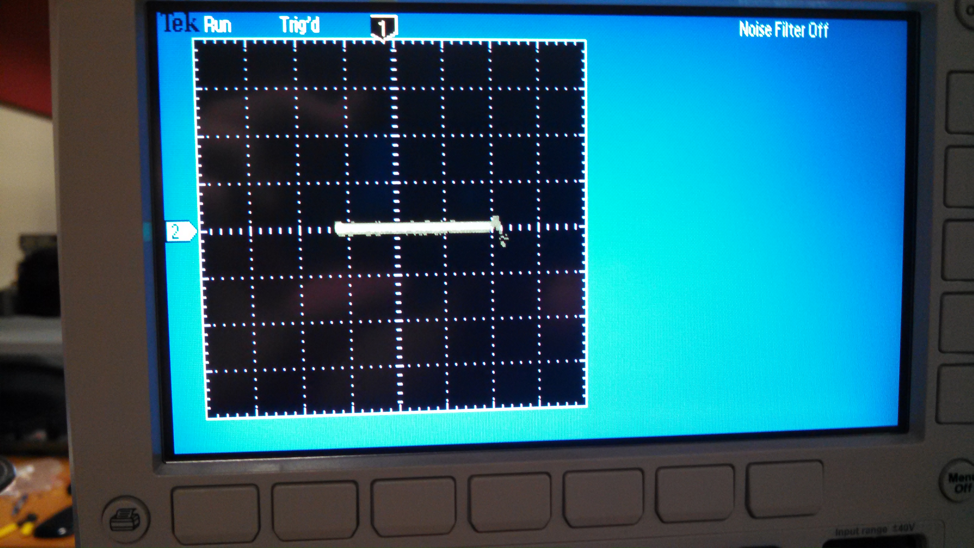
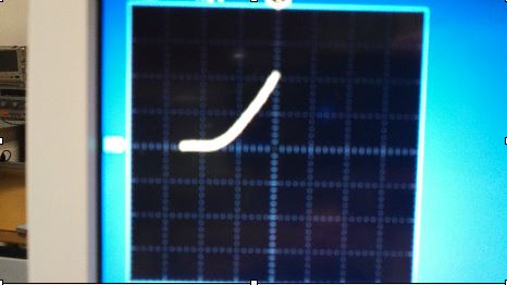
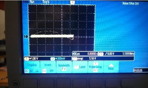
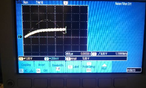
1) Experiment NMOS
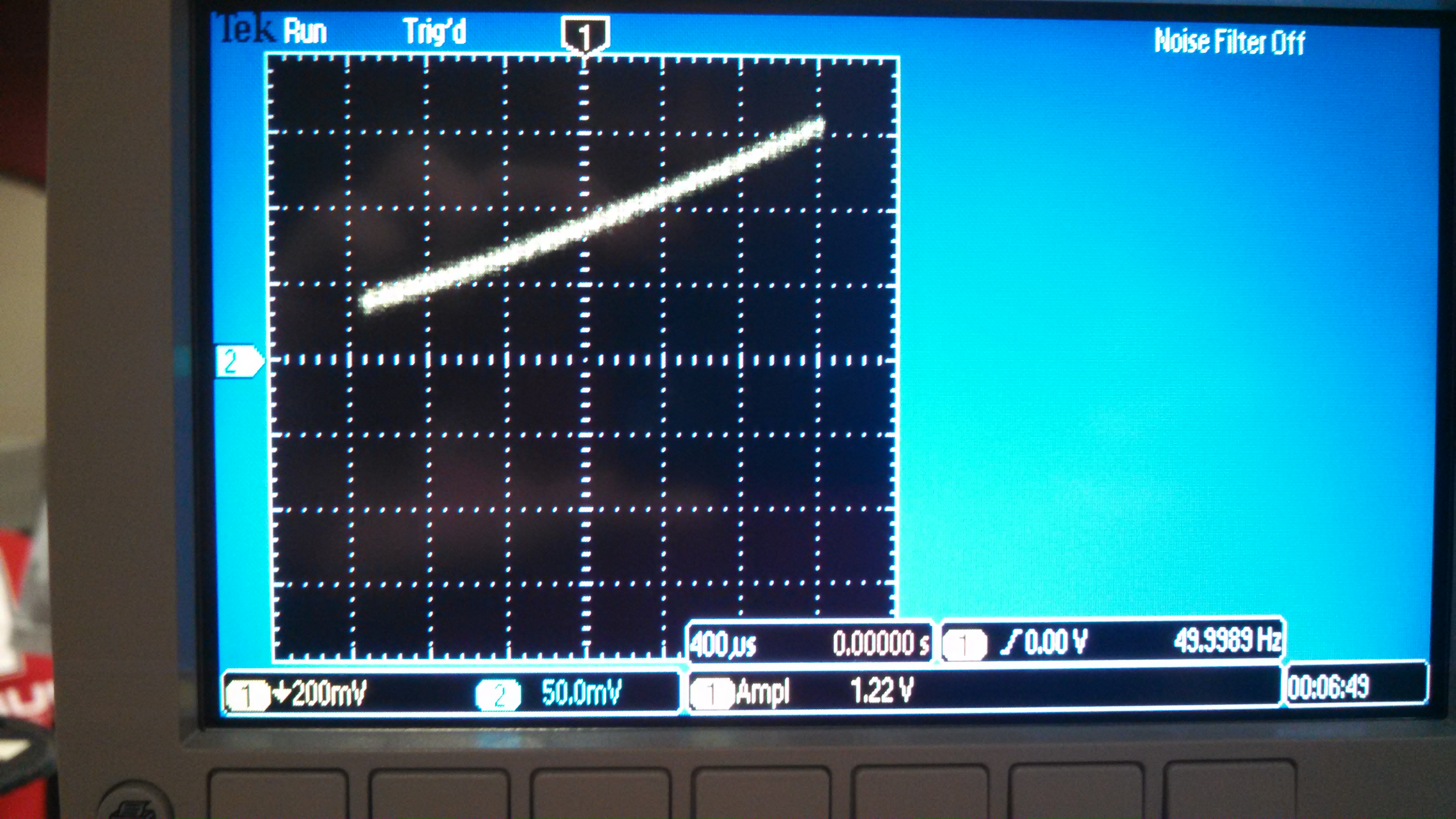
Scope reading
2) Experiment NMOS
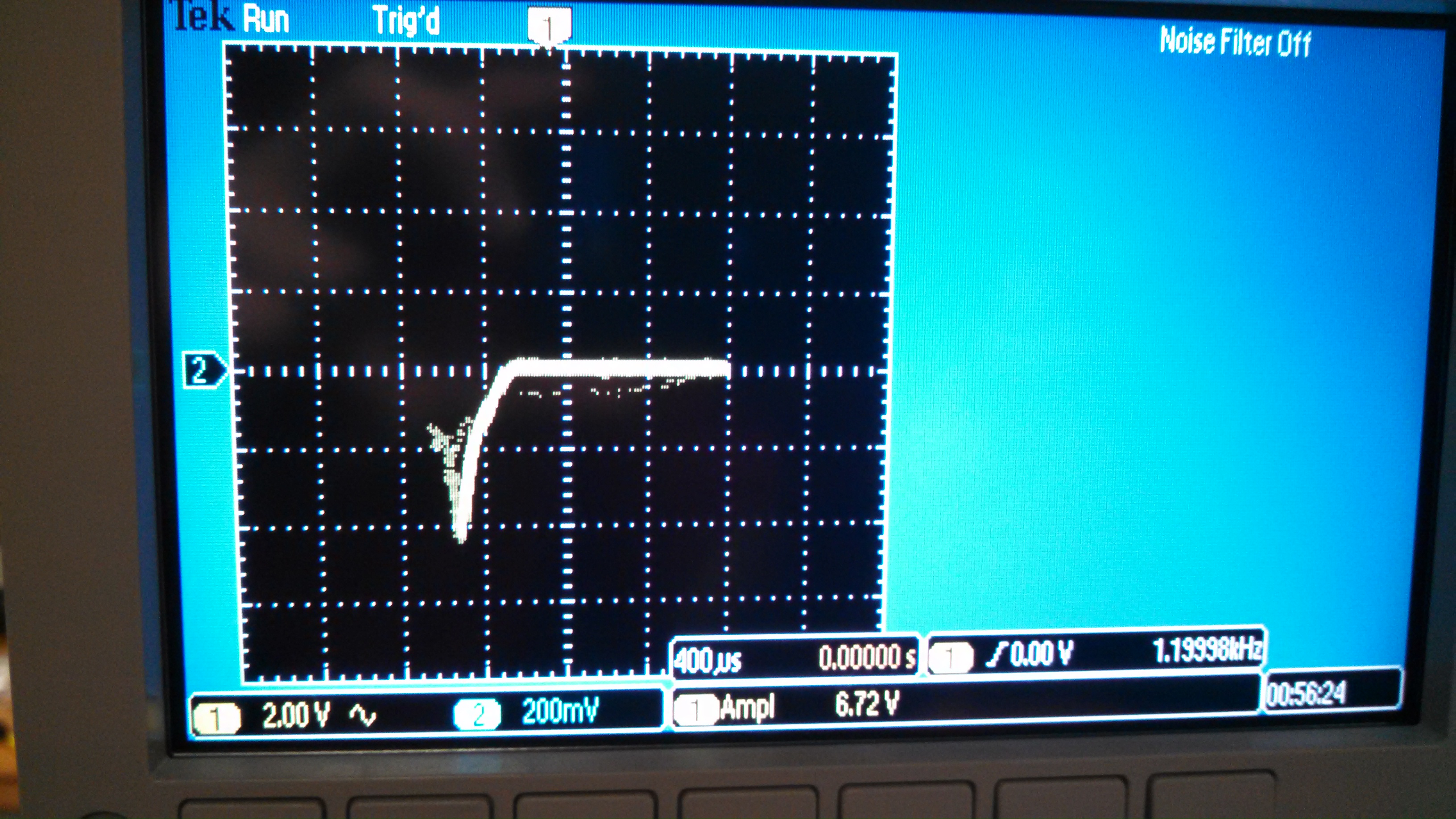
VGS = 1V
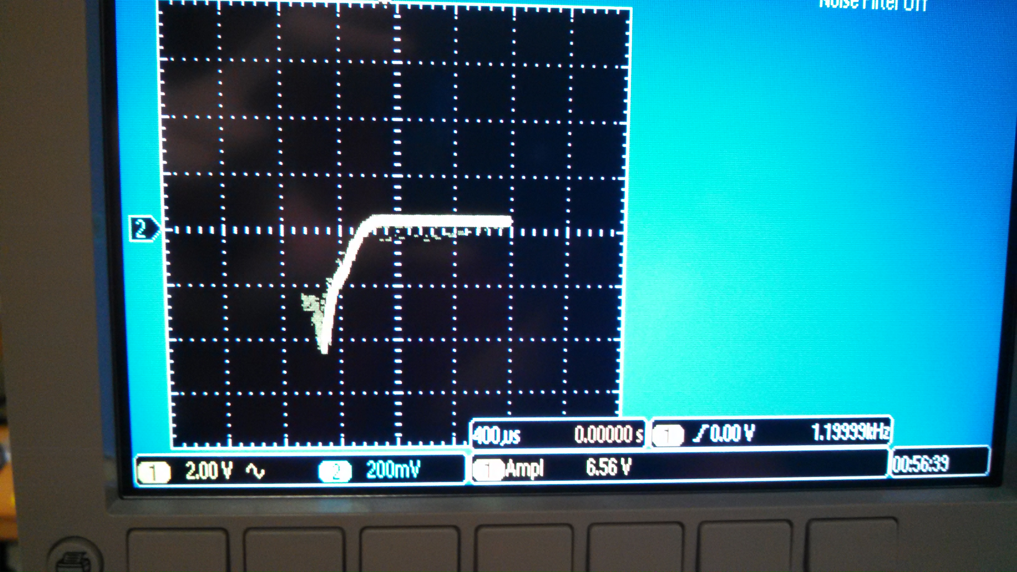
VGS = 2V
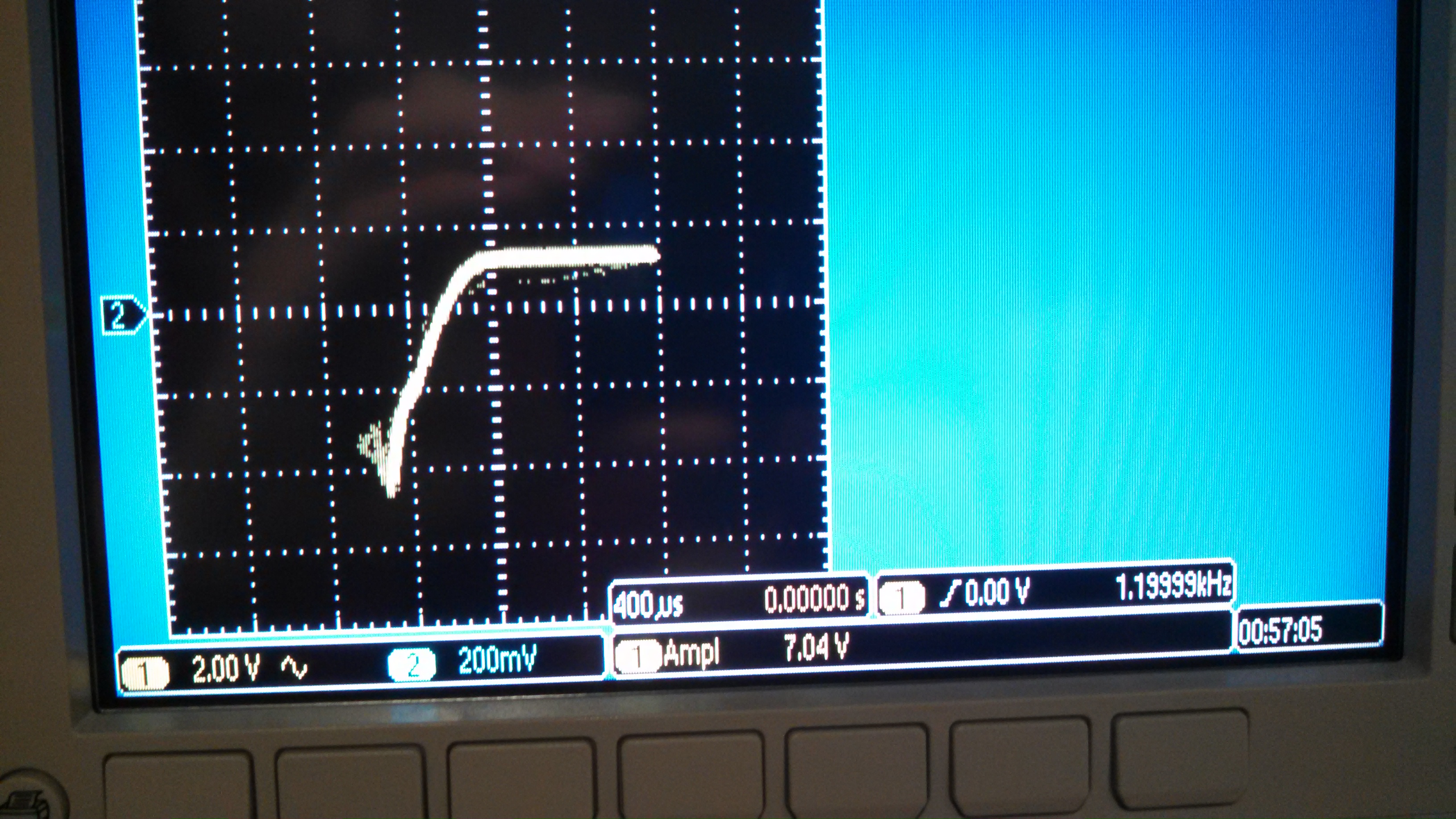
VGS = 3V
VGS = 4V
VGS = 5V
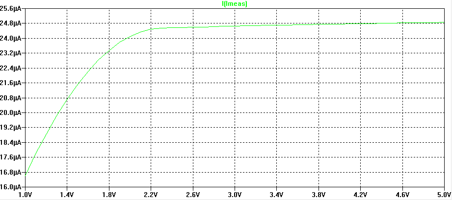
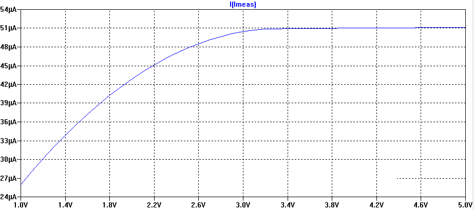
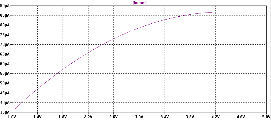
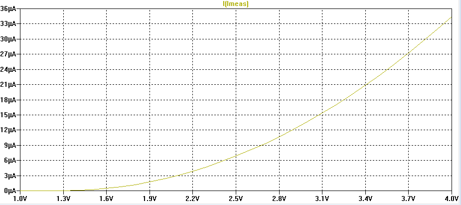
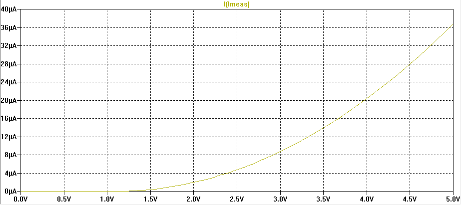
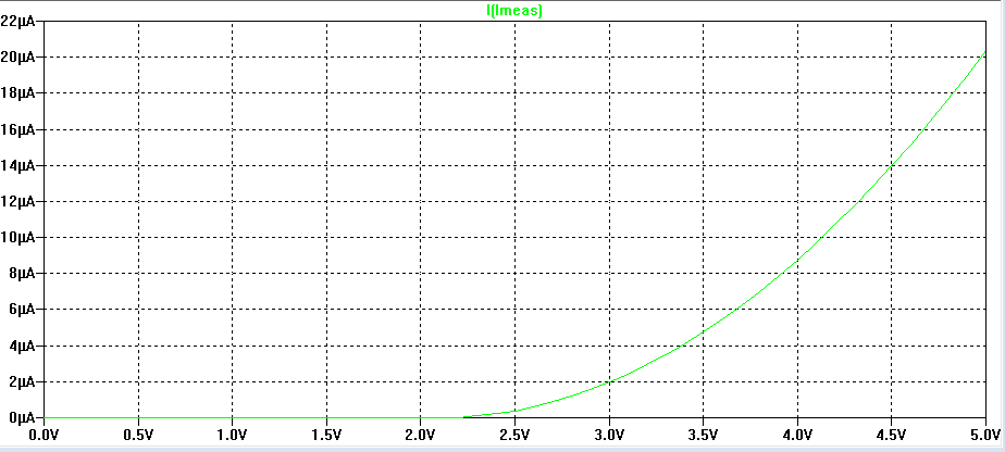
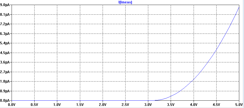
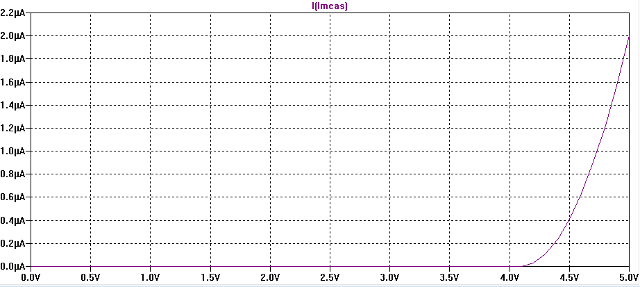
3) Experiment NMOS
VBS = 0
VBS = 1
VBS = 2
VBS = 3
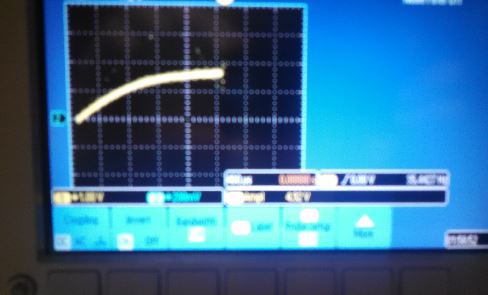
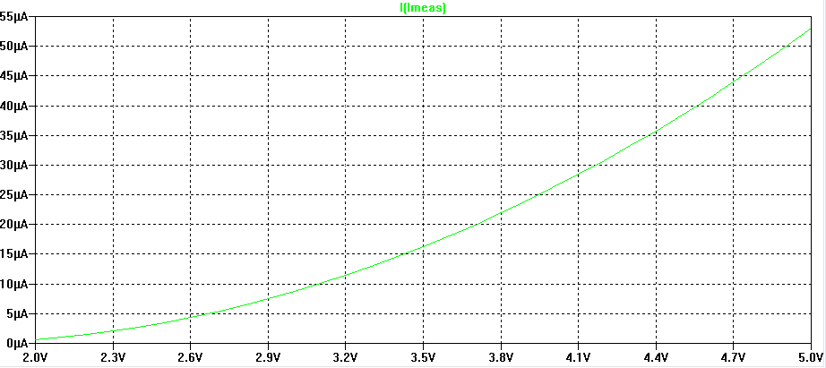
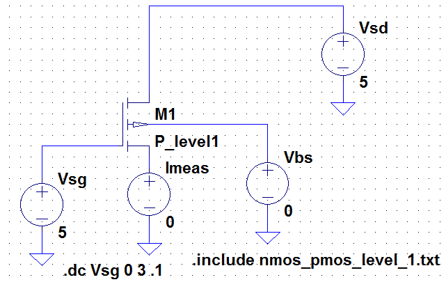
1) Experiment PMOS
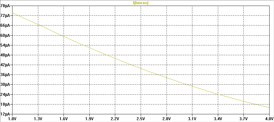
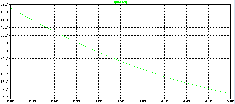
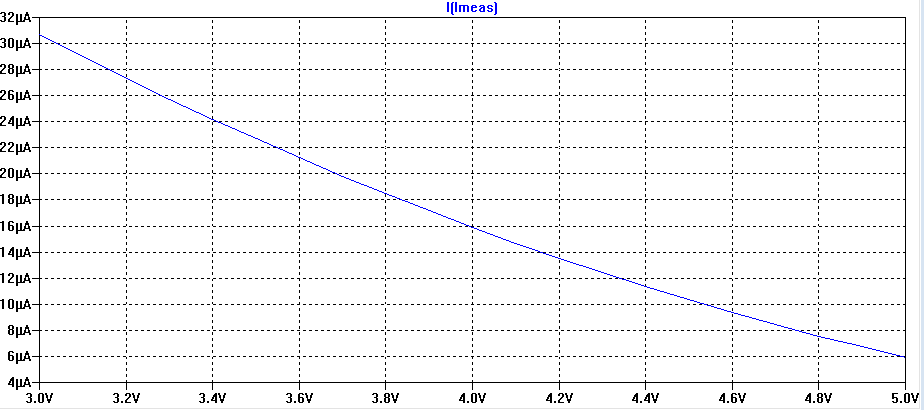
3) Experiment PMOS
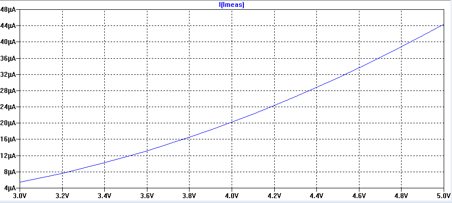
VSG = 5V

VSG = 4V

VSG = 3V
VSG = 2V
VSG = 1V
3) Experiment PMOS
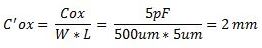
Assuming
that the length of the NMOS is 5 um and its width is 500
um calculate the oxide thickness if Cox (= C'ox*W*L) = 5 pF.
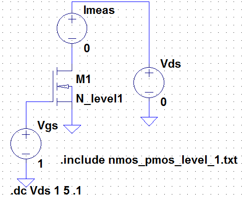
From this data, we create a LTspice model with the following parameters:
.MODEL N_level1 NMOS LEVEL = 1
+ TOX = 1.13E-14
+ VTO = 0.8
+ GAMMA = 1
+ KP = 9.38E-6
*
.MODEL P_level1 PMOS LEVEL = 1
+ TOX = 1.13E-14
+ VTO = 0.8
+ GAMMA = 1
+ KP = 4.8E-6
Using these models, we recreate the 3 experiments in simulation and gather our results.
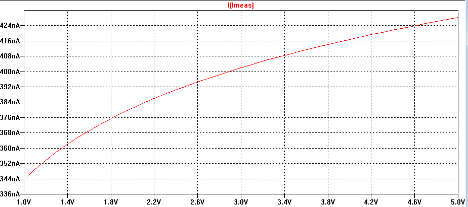
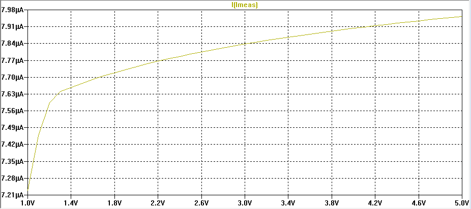
1) Simulation NMOS
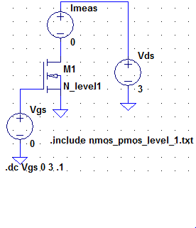
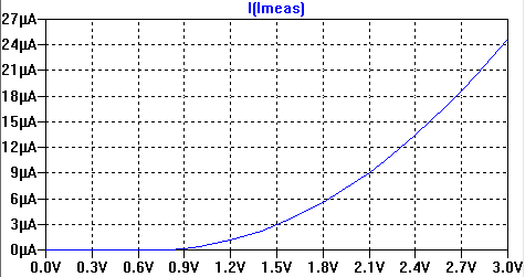
Schematic
Simulation
2) Simulation NMOS
Schematic
VGS = 1V
VGS = 2V
VGS = 3V
VGS = 4V
VGS = 5V
3) Simulation NMOS
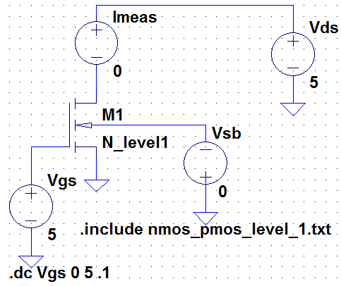
Schematic
VGS varied 0 to 3 V (VSB = 0)
VGS varied 1 to 4 V (VSB = 1)
VGS varied 2 to 5 V (VSB = 2)
VGS varied 3 to 5 V (VSB = 3)
1) Simulation PMOS
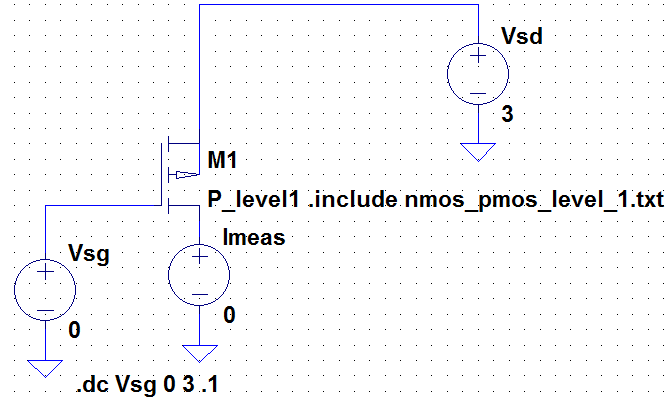
Schematic
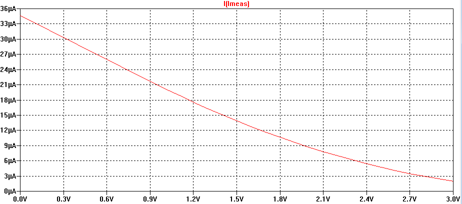
Simulation
2) Simulation PMOS
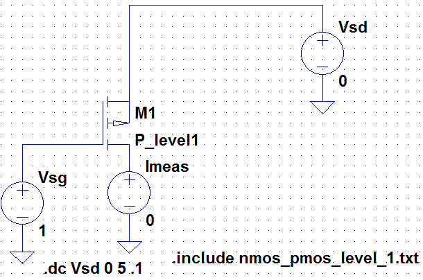
Schematic
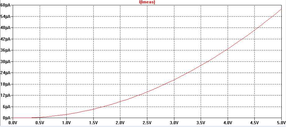
VSG = 1V
VSG = 2V
VSG = 3V
VSG = 4V
VSG = 5V
3) Simulation PMOS
Schematic
VSG varied 0 to 3 V (VBS = 0)
VSG varied 1 to 4 V (VBS = 1)
VSG varied 2 to 5 V (VBS = 2)
VSG varied 3 to 5 V (VBS = 3)
Inverter - Using the chip, we can also build an inverter. The simulation data is provided below:
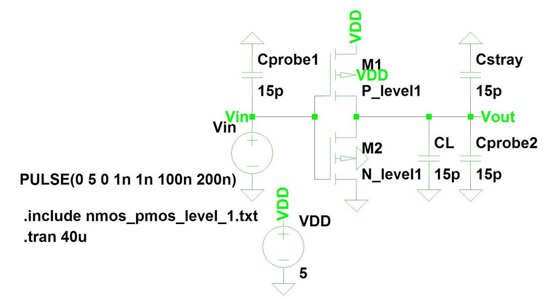
Inverter schematic
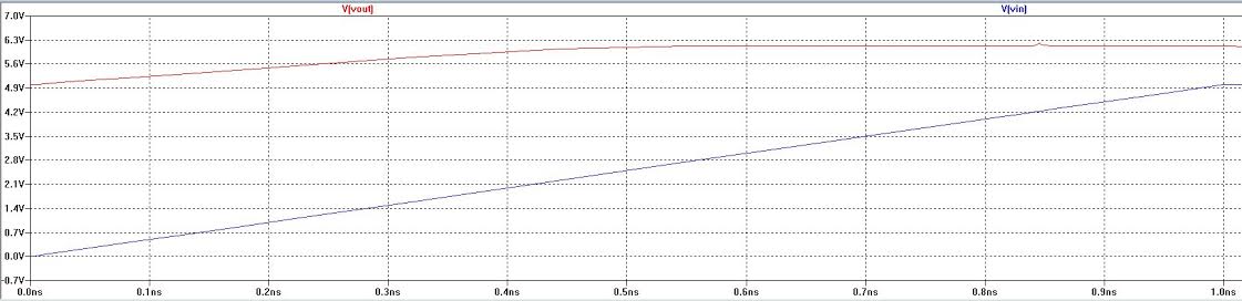
Simulation part 1
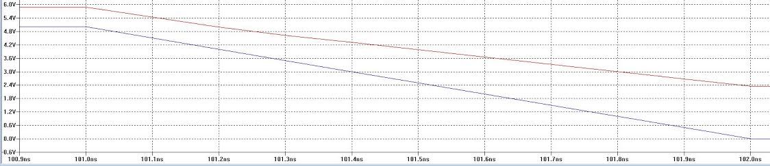
Simulation part 2
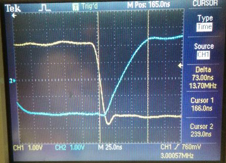
This is the experiemtal data provided from the scope readings:
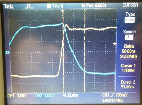
Vin = Yellow (rising), Vout = Blue (falling)
Vin = Yellow (falling), Vout = Blue (rising)