EE 420L - Lab 7
Design of an audio amplifier
The purpose of this lab is to design an audio amplifier, with frequencies between 10Hz to 20kHz, assuming that you can use as many resistors, ZVN3306A transistors, and ZVP3306A transistors as you need along with only one 10 uF capacitor and one 100 uF capacitor. Assume that the supply voltage is 10 V, the input is an audio signal from an MP3 player (and so your amplifier should have at least a few kiloohms input resistance), and the output of your design is connected to an 8-ohm speaker (so, ideally, the output resistance of your amplifier is less than 1 ohm).
Design
Audio amplifiers are needed so that the impedences of the input (audio signal) match the impedence of the output (speaker). Without the audio amplifier, the audio source, i.e. mp3 player plug, would be connected directly to the speaker and becuase the speaker has only a few ohms resistance (8 ohms usually), very little voltage would be applied to the speaker. The audio amplifier amplifies the signal so that a larger voltage swing can be applied to the speaker.
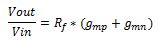
Our audio amplifier is a basic push-pull amplifier whose gain can be calculated with the following equation:
However, because we go not know our exact values for gmp and gmn, we estimate the gain to be in the 1000 range. This assuming Rf to be 10k, however, during the breadboard process, we find that this value to too high as our waveform clips. For this reason, we use a 510 ohm resistor.
Simulation
In simulation we find our real value of 510 ohms to be effective, however, in simulation 510 ohms Rf is too low. Thus we use a value of 510k as Rf in LTspice.
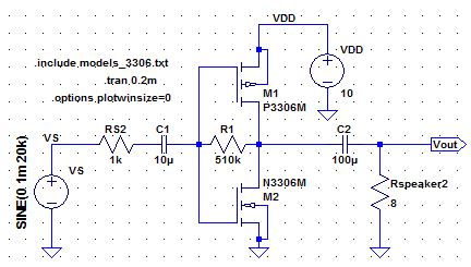
Schematic Waveform
Performance
As stated before, the intial Rf value of 10k was way too high as our Vout waveform kept clipping. For this reason, we used a real Rf value of 510 ohms. Also to note, our input voltage performance value was 4.6V as opposed to our simulation value of 1mV. Another interest is that our frequency is much higher than our design parameter (10Hz to 20kHz). Discussion on these results is provided below the scope results.
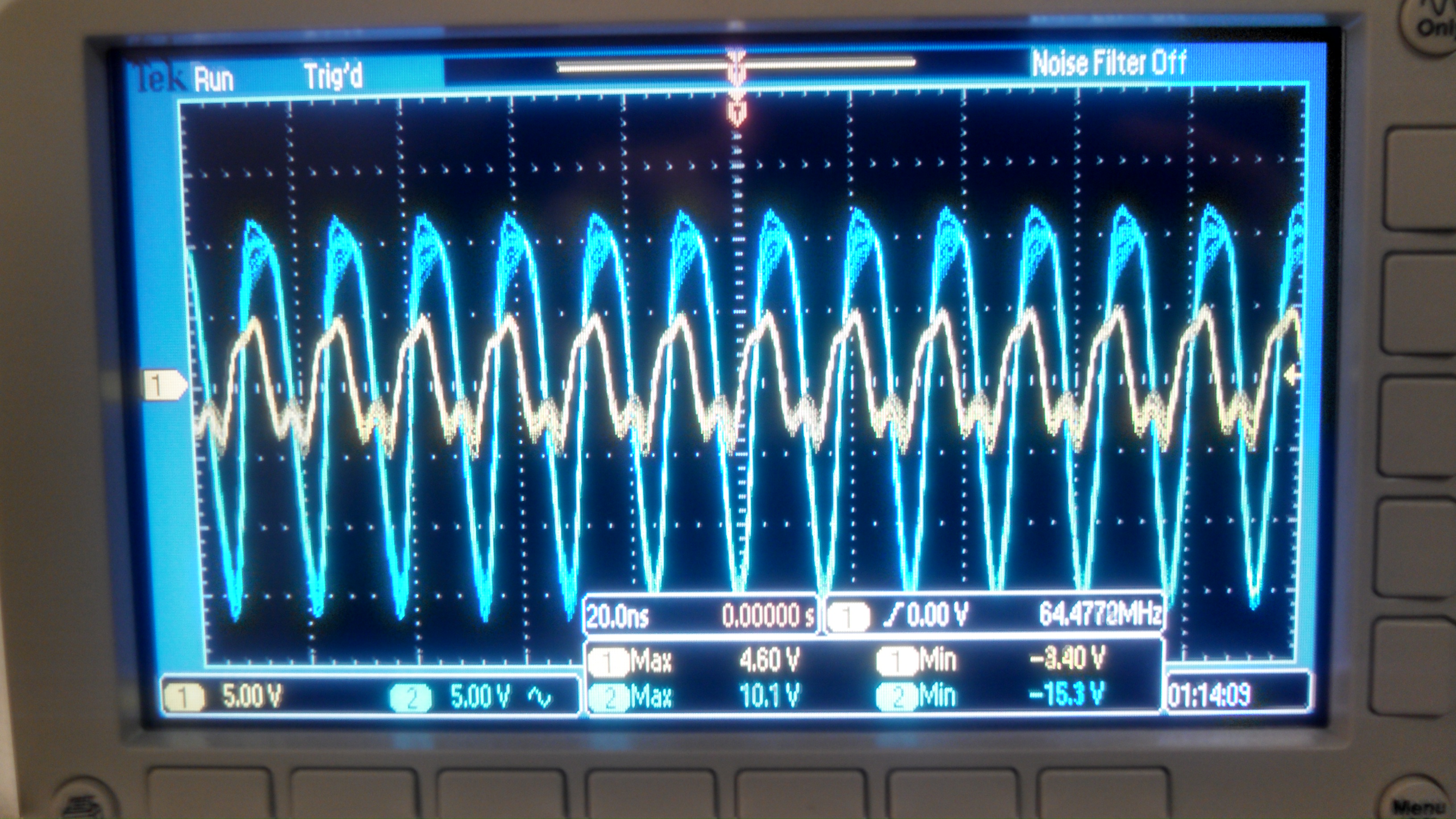
Scope results: Yellow = input audio signal, Blue = amplifier output signal
Output Swing
As displayed from the scope results, we see that our output swing is from +10.1V to -15.3V (25.4 ppV). We believe that the negative voltage swing is higher than the positive voltage swing because the NMOS device might be powered more often than the PMOS device.
Power Dissipation
Power dissipation is how much power is dissipated in the circuit; this can be calculate by the power consumption of the circuit. The power consumption is the product of VDD and the current supplied. Given that our VDD is 10V and our current is about 250mA thus our power dissipation is about 2.5 Watts. This amplifier design is bad for power dissipation because our transistor constantly ran hot.
Input Resistance
The input resistance can range from about 1k to 10k ohms. For our simulation, we used 1k ohms as a low range test while for our input resistance, we determined the value to be closer to 10k ohms.
Output Resistance
We use a standard 8 Ohm speaker for our audio amplifier thus our output resistance is 8 Ohms.