EE 420L - Lab 5
Op-amps III, the op-amp integrator
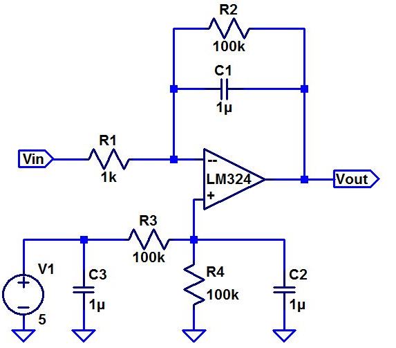
(Q) Calculate the frequency response of the following circuit. Ensure you show your clear hand calculations.
Integrator op-amp topology
(A) For calculating the frequency responce of the op-amp, we focus on the ac part of the circuit, thus, our circuit simplifies to this:
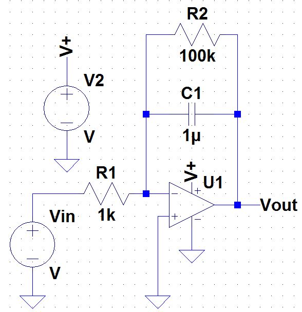
AC part of the circuit
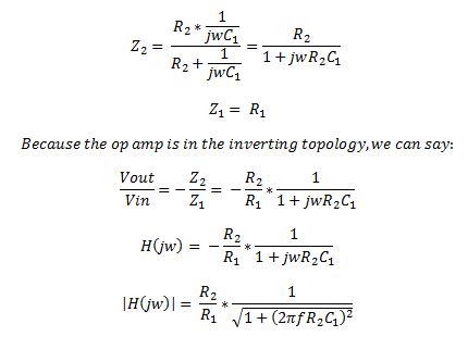
H(jw) is the frequency responce of the systems
(Q) What can you neglect to simplify the calculation?
(A) We can neglect the R2 resistor for these calculations because the op amp will still be the integration (and inverting) topology. Not only that, the R2 resistor is only used for a DC feedback path but since we are only looking for the AC frequecny responce, we can neglect R2 for these calculations. In our case, the point is moot as our DC Vp = 2.5 and our DC Vm = 2.5 so our DC gain would be 1 in any case which wouldn't disturb our calculations anyway. And if our voltages are the same, there is no voltage drop across R1 meaning there would be no DC gain.
(Q) Does the circuit work if you remove the 100k? Why or why not?
(A) The 100k resistor, R2, is only used as a DC feedback responce. If it is removed, DC current will have no path as the capacitor acts like an open for DC current. Removing R2 also esentially sets R2 = infinity, making our DC gain infinity which in reality would only saturate it to either our 0v or 5v rain. Thus for DC analysis, it is important for setting a stable DC gain.
(Q) Does the 100k have much of an effect on the frequency response?
(A) As stated earlier, the 100k resistor is only used for DC feedback and DC gain, which doesn't matter too much for AC analysis. The resistor is set to a high resistance so that most (ideally all) of the AC current flows through the capacitor, causing the capacitor to charge and discharge, which produces our triangle output waveform.
(Q) Verify your calculations with experimental results.
(A) The following are pictures from our oscilloscope with the circuit in the integration topology.(Yellow = Vin, Blue = Vout)
Unity gain at 10KHz.
Scope output
(Q) Show, at the unity-gain frequency of the integrator, that the input and the output have the same peak values. Is the phase shift between the input and the output what you expect? Why or why not?
(A) We expect the phase shift to be +90 degrees from our earlier calculations of frequency responce. In our frequecncy responce, we produced j which translates to 90 degrees, thus our 90 degree phase shift is to be expected.
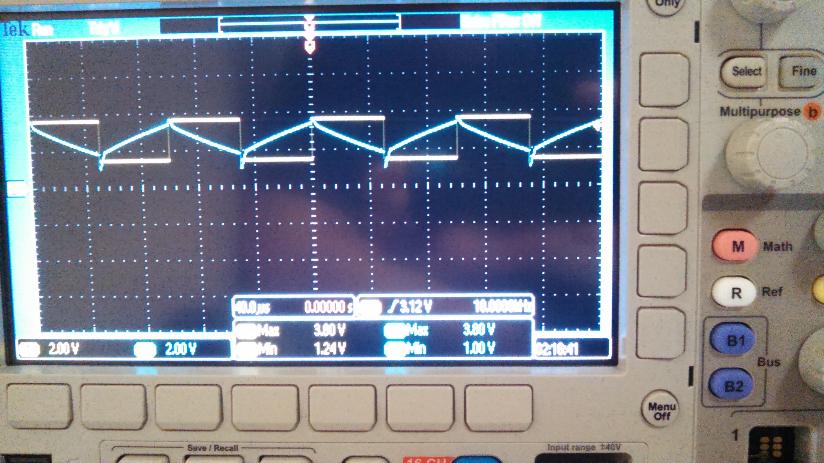
(Q) Next, design, simulate, and build a square-wave to triangle wave generation circuit. Assume the input/output frequency is 10 kHz and the output ramp must swing from 1 to 4 V centered around 2.5 V. Show all calculations and discuss the trade-offs (capacitor and resistor values, input peak, min, and average, etc.)
(A) The following are our results:
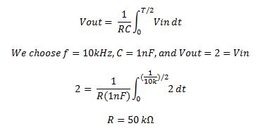
Calculations for determining R
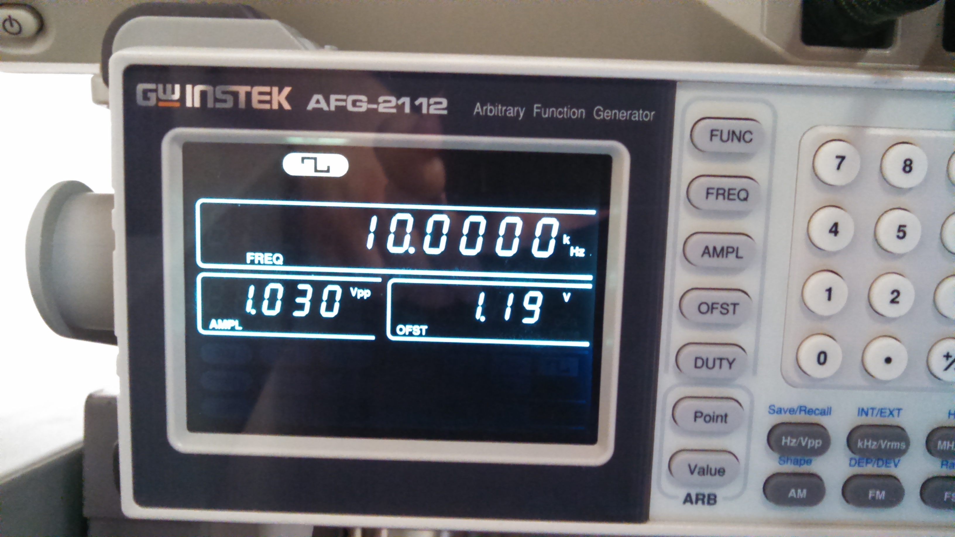
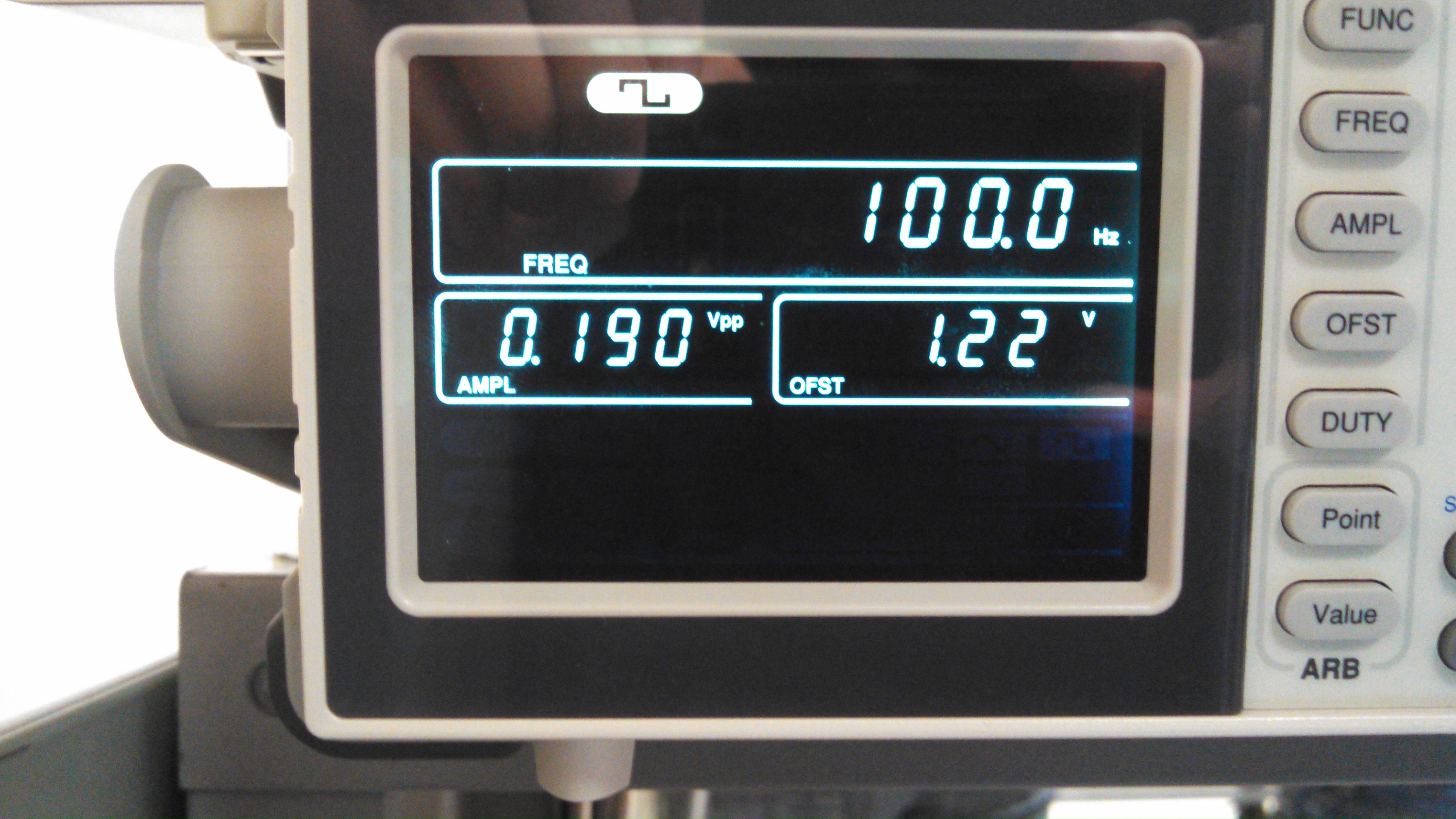
frequency = 10k, Vin = 1.030V, DC Offset = 1.19V
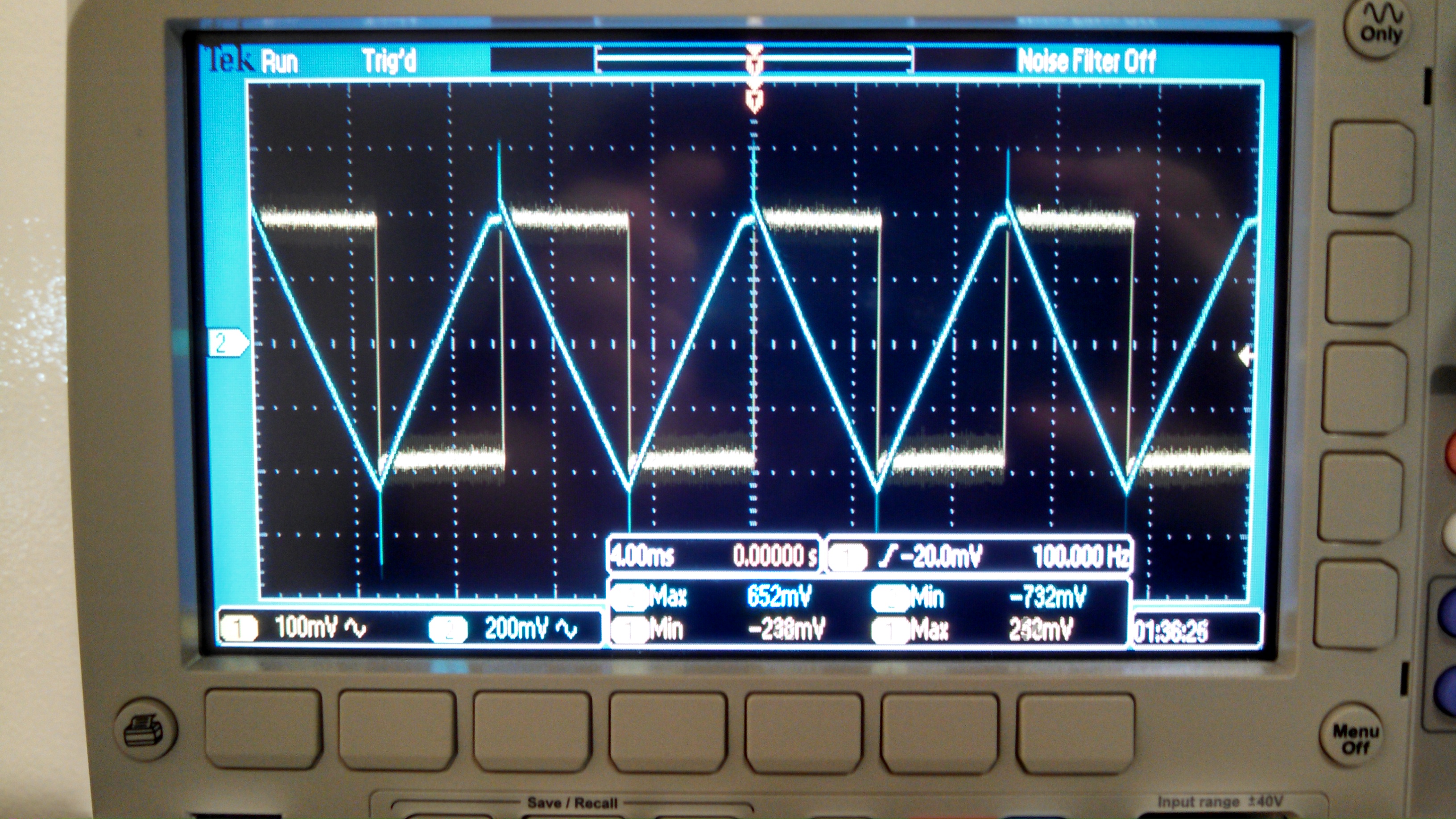
Unity gain at 10KHz
Tradeoffs: A larger R will cause a larger DC gain which will make it harder to center our Vout at 2.5v as the gain will push Vout toward one of our rails of 0v or 5v. However, a large R is useful as the phase change will close to +90 degrees. Close, but still a little off as we can see from the scope output.