EE 420L - Lab 3
Op-amps I, basic topologies, finite gain, and offset
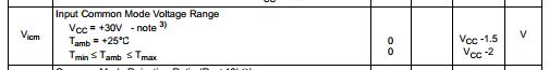
(Q) Knowing the non-inverting input, Vp, is at the same potential as the inverting input, Vm, (called the common-mode voltage, VCM) what are the maximum and minimum allowable common-mode voltages?
(A) From the data sheet, we can see that the minimum input common mode voltage is 0V and the maximum voltage is Vcc - 1.5. Because our Vcc = 5V, our maximum common mode voltage is 3.5V and our minimum is 0v.
-----------------------------------------------------------------------------
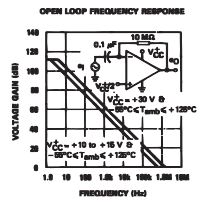
(Q) What is a good estimate for the op-amp's open-loop gain?
(A) This information can be found from three (3) sources:
i) As indicated, the open loop gain is typically 100V/mV, this converts to 100k V/V.
ii) We also could have recieved this knowelge from the front of the data sheet as indicated below:

20log(x) = 100 ----> x = 5 ----> 10^(5) = 100k V/V.
iii) Lasly, we can also find our gain as a function of frequency. Given our frequency to be sufficiently low for these experiments, we can say our gain is 100dB or 100k V/V.
-----------------------------------------------------------------------------
(Q) What is a good estimate for the offset voltage? For worst case design what value would you use?
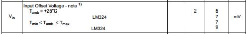
(A) From the data sheet, we can see that the average offset voltage is 2mV and for a worst case senerio, we would use the maximum value of 9mV.
EXPERIMENT 1
For the following questions, we use this the circuit below:
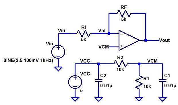
(Q) What is the common-mode voltage, VCM? Does VCM change? Why or why not?
(A) VCM is 2.5V because of the voltage divider circuit. The 2.5V doesn't change because the small capacitors act like an AC short, so if we have any 'wiggling', it discharges through the capacitors and the 2.5 DC is preserved.
-----------------------------------------------------------------------------
(Q) What is the ideal closed-loop gain?
(A) This answer has two parts, one for DC and one for AC.
i) The DC gain is 1, this is because we have 2.5VDC going in the invertering terminal (-) and 2.5VDC going in the non-inverting terminal (+). Because their is no 'difference' between these two vaules, our gain is unity or 1 V/V.
ii) The AC gain is -1, this is because the AC source goes into the inverting terminal (-) and the non-inverting terminal is 0v (DC voltage source = AC ground). Thus, the op-amp is in the inverting topology which means our gain is -R2/R1 = -5k/5k = -1.
-----------------------------------------------------------------------------
(Q) What is the output swing and what is it centered around? What happens if the input isn't centered around around VCM, that is, 2.5 V?
(A) The output swing is centered around 2.5V because this is our VCM and our output swing is the 100mV AC signal. If our swing isn't centered around 2.5V, we might not have enough 'room' for our signal to swing and our output could become saturated. For example, if R2 = 20k, our swing would be -400mV (gain (-4) x input voltage (100mV) = -400mV). However, none of this would saturate because we are still centered. If instead, our VCM is set to 0V with R2 = 20k, our DC gain would be -4V (gain (-4) x input (2.5V) = -10V) and our AC gain would be -400mV meaning our offset would be -10v. Because out Vcc is 5V and -Vcc is 0V, we are only allowed to swing between those two values, thus is we are centered at -10V, we are completely saturated and never see our signal. In this way, our DC vaules center us and determine how much room our AC signal has to swing.
-----------------------------------------------------------------------------
(Q) What is the maximum allowable input signal amplitude? Why?
(A) Because Vcc = 5 and -Vcc = 0, out output can only swing between those two values. If our ouput goes beyond those boundaries, our signal become saturated and clips off.Because we are centered at 2.5V, this means our maximum output swing is +2.5v (2.5 + 2.5 = 5) and -2.5v (-2.5 + 2.5 = 0). And, because our gain is -1, this mean our maximum input signal amplitude is 2.5V, theoretically, practically, we will probably never reach that value.
-----------------------------------------------------------------------------
(Q) What is the maximum allowable input signal if the magnitude of the gain is increased to 10? Why?
(A) If our gain is increased to 10, we can still only swing between Vcc = 5 and -Vcc = 0. And because we are centered at 2.5V, our signal can only swing 2.5V. This means our max input is (input) x 10 = 2.5 which makes our max input signal 250mV.
-----------------------------------------------------------------------------
(Q) What is the point of the 0.01 uF capacitors from VCC and VCM to ground? Are these values critical or could 0.1 uF, 1,000 pF, 1 uF, etc. capacitors be used?
(A) As stated earlier, the capacitor are only there act as a chort for any AC wiggle and keep our input as 2.5VDC. It is good to have small capacitors so that they charge and discharge quickly as not to steal any voltage from our DC source.
-----------------------------------------------------------------------------
(Q) The data sheet shows that this op-amp has an input bias current that flows out of the op-amp's inputs of typically 20 nA. This current flows out of both the non-inverting and inverting inputs through the resistors connected to these inputs. Show how the operation of the circuit can be effected if, for example, R1 and R2, are much larger.
(A) Because this input bias current flows out of our inverting and non-inverting terminals, it also flows through our resistors. By Ohms Law, this means creates a small voltage. In our experiment, 20nA*(5k || 5k) = 50uV, which makes our VCM 2.5V + 50uV, not a noticable change. However, if our resistors were larger, say 5M, then our VCM would be 20nA*(5M || 5M) = 0.05V + 2.5 = 2.505.
-----------------------------------------------------------------------------
EXPERIMENT 2
For the following questions, we use this the circuit below:
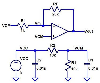
(Q) Explain how the following circuit can be used to measure the op-amp's offset voltage.
(A) We can use this circuit to measure the offset voltage of the op-amp by measureing the difference between the inverting terminal and the non-inverting terminal. However, because our op-amp has a gain of 20, any difference we measure must be divided by 20 to obtain the actual value or:
offset voltage = (|Vp-Vm|)/A
With Vn = voltage at inverting terminal, Vp = voltage at non-inverting terminal, and A = gain.
Repeating this for four different op-amps, we put the results in a table below:
| Op-Amp | Vn | Vp | |Vn-Vp| | |Vn-Vp|/A |
| 1 | 7 mV | 6.7 mV | 0.3 mV | 15 uV |
| 2 | 11.2 mV | 11.5 mV | 0.3 mV | 15 uV |
| 3 | 7.4 mV | 7.2 mV | 0.2 mV | 10 uV |
| 4 | 2 mV | 2.8 mV | 0.8 mV | 40 uV |