Designing a
Band-Gap Voltage Reference
EE 420L
Engineering Electronics II
Author:
Matthew Meza
Email:
mezam11@unlv.nevada.edu
May
8th, 2015
Project Guidelines and Requirements
Using
as many diodes, resistors, and capacitors as needed, along with two
CD4007 chips from the same production
lot
(see date code on the top of chip) to ensure current mirrors are
possible, design and build a bandgap voltage
reference
(BGR). Your report, in html, should detail your design considerations,
simulation results (using the models
you
generated in lab 8), and measured results showing the BGR's
performance (how the reference voltage changes
with
VDD). It
would be good, but it's not required, if you could also characterize
the BGR performance with
temperature.
Your report is due
at the end of lab on Friday, May 8. Access to your CMOSedu.com
accounts
will
be removed at this time.
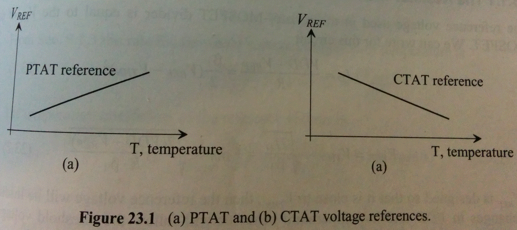
Introduction to Voltage References
A voltage refernce is a
circuit used to generate a fixed voltage which
is often referred to as 'Vref'. The fixed
voltage 'Vref' is independent
of the power supply voltage (VDD),
temperature, and process variations. More
specifically, a bandgap
reference is a type of voltage reference which
uses both a proportional
to absolute
temperature (PTAT) quality and
a complementary
to ablsole
termparture (CTAT)
quality. When a voltage
reference has a PTAT quality
it means that the reference voltage
increases with increasing temperature; while
a voltage reference that has
a CTAT quality means that the refernece
voltage decreases with increasing
temperature. Since the
bandgap voltage reference incorporates both
qualities, the net change in the voltage
reference with increasing
temperature is ideally zero! Shown below is
figure 23.1 from "CMOS
Circuit
Design,
Layout,
and Simulation", by R.
Jacob Baker, which illustrates PTAT and
CTAT voltage references.
Design Considerations
For the Band-Gap Reference
(BGR) design, a diode-referenced
self-biasing circuit will be used for the CTAT
quality and thermal
voltage-referenced self biasing circuit will be
used for the PTAT quality. Ideally, a cascode
structure should be used
(higher output resistance) to force the same
current through each branch of of the
reference as seen below!

Unfortunately, only two
CD4007 chips can be used which significantly
limits the design since the BGR with the
cascode structure, shown
above, cannot be implemented! For this project
a regular current mirror must be used to
design the BGR which will
have reduced performance as compared to the
previously shown design. Shown below is the
BGR using a regular current
mirror where K = 8 which is the number of
diodes used in parallel. The two left most
branches (current mirror) is
referred to as a Thermal
Voltage-Referenced Self Biasing circuit which provides the
PTAT quality. Using K diodes
in parallel in the middle branch increases
the current flowing in the branch such that
the current flowing through
the reference is non-zero. The same effect
could be realized by increasing the
MOSFETS size on the leftmost
branch. The PTAT current generated from
the current mirror is then driven into
a resistive load R*L (PTAT
quality) and a diode (CTAT quality) to
create a voltage reference which ideally does
not change with temperature,
VDD variations, or process variations!

The hand calculations to find
the appropriate resistance value (R) and
length (L) can be seen below:

In our build and
simuluations, we used PNP BJT's which were grounded at
the base and collector instead of a diode.
Simulations
Below is our circuit in
LT-Spice along with simulations!
Click on this picture for the
full image!

VREF
VS VDD
with variations in temperature

(click on pictures for full size)
|
VREF
VS VDD
ZOOM

|
IREF
VS VDD
with variations in temperature

|
IREF
VS VDD
ZOOM

|
Note: The simulation models
must have a lambda value to be accurate. A
lambda value of 0.5 was used in the model.
From our simulation results
we see the voltage reference changes
approximately 282mV per 1V increase in VDD!
In addition, from simulations
we see that the current changes
approximately 442nA per 1V increas in VDD!
Experimental
Shown below is a picture of
the built BGR circuit. Notice the big blue
resistor on the top right; it is used as a
start up circuit by leaking a
small amount of current into the NMOS
gates so that the BGR circuit is in operation.

After measuring the voltage
and current for several VDD, we graphed the
data in Excel.
The graph below plots the
changes in Vref with varying VDD. From our
experimental data, Vref increases
approximately 220mV per 1V in
VDD. This is better than our simulation
value!

The graph below plots the
changes in Iref with varying VDD. From our
experimental data, Iref increases
approximately 350nA per 1V in
VDD. This is also better than our
simulation value!

Conclusion
Although the changes in VRef
and Iref are not as small as we would
like, we can see first hand that the BGR does
work. Being limited to only 2
CD4007 chips definitly inhibits the
possible performance of the BGR. As stated
above, it would be ideal to
have a cascoded current mirror for a higher
output resistance. Nonetheless, the project
proved to be helpful in
seeing how process variations can also change
the performance of a BGR. Overall I score
this Lab-Project a 10/10.
Return
to EE 420 Labs