Lab 9 - ECE 420L
Authored
by Steven Leung
leungs@unlv.nevada.edu
4/17/15
Lab
description
The
main purpose of this lab is to be able to generate bias currents for a
NMOS and PMOS devices in the CD4007 chip. This is done using a
betamultipler and NMOS/PMOS current mirrors.
Pre-lab work
- This lab will use the level=1 MOSFET model created in lab 8 and, again, the MOSFETs in the CD4007.pdf CMOS transistor array.
- Design and simulate the operation of a BMR that biases the NMOS devices so that they have a gm of 20 uA/V
- Use a simple (big) resistor to VDD for the start-up circuit (explain how the addition of a resistor ensures start-up).
- When
the BMR is operating the current in the big resistor should be much
smaller than the current flowing in each branch of the BMR
- Write-up,
similar to a homework assignment, your design calculations and
simulation results. (This will count as the pre-lab quiz.)
- Ensure that you show the following in what you turn in:
- Hand calculations
- Operation as VDD is swept from 0 to 10 V
- Vbiasn
should stabilize (be constant) after VDD hits a minimum value (estimate
this value of VDD assuming VGS/VSG is a threshold voltage and
VDS,sat/VSD,sat is zero).
- Vbiasp should follow VDD after VDD hits a minimum value (show this in simulations)
- Unstable operation if too much capacitance is shunting the BMR's resistor (see bottom of page 630)
- Comments comparing the hand calculations with the simulation results
Design
The design of the betamultipler was done in the prelab and can be see here.
Expeimental simulations
For
the following plots below, they are generated either by measuring the
resistance across the resistor in the betamultipler or measuring the
current through one of the transistors using a multimeter. The data is
measured over a range of data and then inputted into excel for
plotting. The exact values for each experiment can be see in the excel
document here.
VDD v. ID
Below
if the current plot of the betamultiplier. This was taken by
measuring the voltage across the 50k resistor (see prelab) and thendividing that by 50k.

It
can be seen that this curve does not flatten out at higher voltages but
this result is similar to the simulation results.
VDD v. Vbiasn /Vbiasp:

VDD v. Vbiasn | 
VDD v. Vbiasp |
From
the graphs above, it can be seen that the voltage of Vbiasn with
respect to VDD remains close to constant after a certain mimumim VDD
voltage and the voltage of Vbiasp follows VDD after a certain voltage.
This is beucase the voltage of VGS needs to be constant for the
betamultiplier to supply a constant current regaredless of the power
supply voltage. However for the PMOS, if we increase VDD, we are at the
same time increasing VSG which would mean more current.
Using the beta multiplier to connect a NMOS/PMOS device:
This
is done by taking the voltage of Vbiasn to the gate of a NMOS, ground
it's soure and put the drain to VDD. This will ensure that VGS (main
controlling part of ID) will remain the same for the NMOS in the
betamultiplier and the NMOS device to be used. On the other hand, it
will be harder to use the same concept for a PMOS device becuase if the
source of the PMOS is tied to VDD and the gate is tied to Vbiasp
(constant voltage), as VDD increases, the current through the
transistor will start to increase. Therefore, we will typically need
another stage to get a constant current flowing through the PMOS
(usually bias it with a NMOS device)
Below includes plots of using Vbiasn and Vbiasp to bias NMOS and PMOS transistors.

NMOS device | 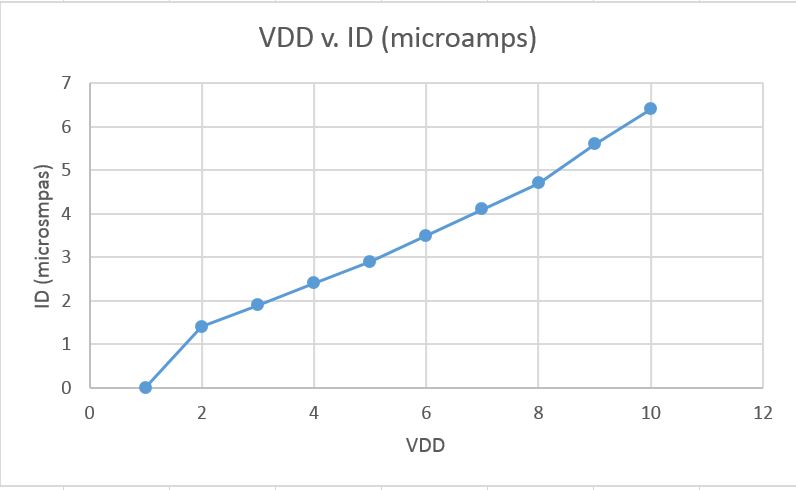
PMOS device |
From
the plots above, we can see that the current throught the NMOS device
is close to stright and the current through the PMOS device increases
with respect to VDD as we prediced.
Using current mirrors to drive 2 gate drain connected devices (cascoding)
To
use current mirrors to drive 2 gate drain connected devices, first
we will take Vbiasp to the gate of a PMOS and then the source to VDD
(just like in the example above). The drain of the PMOS is connected in
series to 2 gate drain connected NMOSs. The same idea is used for the 2
gate drain connected PMOS case but instead Vbiasn will be connected to
the gate and add 2 gate drain connected PMOS from VDD to the drain of
the NMOS. The purpose of this is to increase the output
resistance of the circuit and therefore flatten the curve out.
The plots for the NMOS/PMOS cascode are shown below.

PMOS cascode | 
NMOS cascode |
From
the hand calculations, we should see that after the circuit receives a
minimum VDD voltage, the current should not change much with respect to
increasing VDD. This is the case for the NMOS current mirror and PMOS
cascode but not for the PMOS current mirror or NMOS cascde. The reason
for this may be that in hand calculations, we are assuming that there
is perfect matching and no effect from noise. However, when actually
building these circuits, these other effects can make the circuit not
work.
Add
a return to the listing of your labs