Lab 6 - EE 420L
Authored
by Steven Leung
Today 3/15/15
Leungs@unlv.nevada.edu
Lab
description:
The
main purpose of this lab is to understand the different types of
amplifier configurations such as common drain, common source, and
common gate using NMOS PMOS transistors. Lastly, this lab is go over
some basic characteristics of push pull amplifiers
Pre-lab work
- This lab will utilize the ZVN3306A and ZVP3306A MOSFETs.
- Review these datasheets and become familiar with these transistors.
- Verify that the simulations seen in lab6_sims.zip reasonably model the behavior of the transistors' ID v. VGS, ID v. VDS, and gm v. VGS curves.
- Finally, watch the video single_stage_amps and review single_stage_amps.pdf
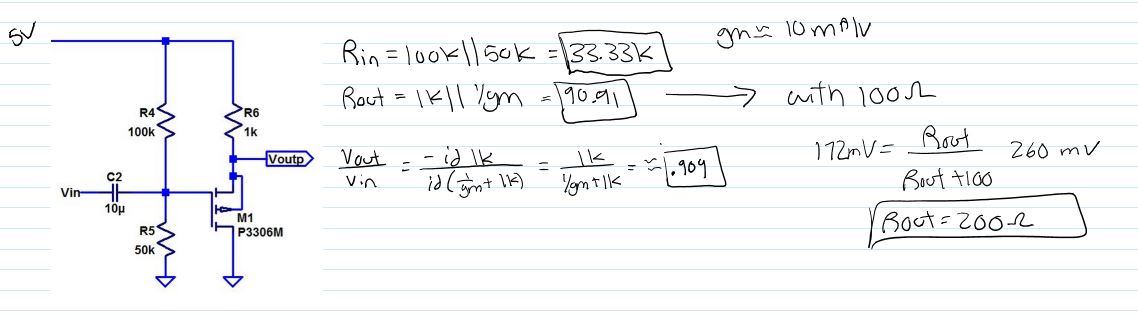
Experiment 1: Common drain
Note:
When using electrolytic capacitors for this experiment the positive
side is connected to the gate because at the node that the input is
applied, it is just an AC wiggle around 0 but at the gate, there is
some DC offset caused by VDD.
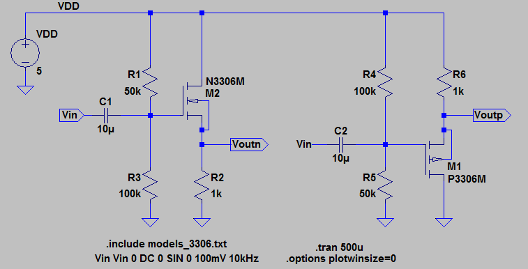
A common drain amplifier means that the drain is common to the input
and output. For this amplifier, we will have the input at the gate and
the output at the source. We can see that the voltage at the drain
is not changing therefore naming it a common drain. The input
resistance can be calculated as the resistance looking into the input
which for both PMOS and NMOS case will be the two resistors connected
to the gate in parallel. The output resistance can be calculated in a
similar fashion as the source resistance in parallel with 1/gm. The
gain can be calculated by writing an equation for Vin and Vout and
taking Vout/Vin to find the gain. (see calculations below) The values
of gm is read off a data sheet and for this lab, we will use a value of
20mA/V for a NMOS transistor and 10kmA/V for a PMOS transistor.
Although these values for gm change with respect to drain current and
VSG or VGS voltage, in order to save time, we will use a rough estimate
of gm for the circuits in this lab.
The reason why the input is centered around 0 while the output has some
DC offset is becuase in order to bias the transistor in saturation,
there is a DC voltage at the output that is not zero. The value of this
offset can be calculated by solving the square law equations. When
adding the DC and AC components, we get the output to have the
calculated gain swing around the biased DC voltage. Since this
amplifier has a gain fo about one, one practical application of this
amplifier is that it can be used as a level shifter meaning that it can
be used to shift an signal to a desired DC voltage while keeping the
amplitude of the signal unchanged.
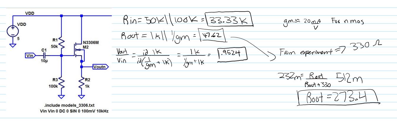
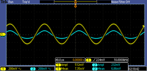
Common drain w/NMOS
Common drain
w/PMOS
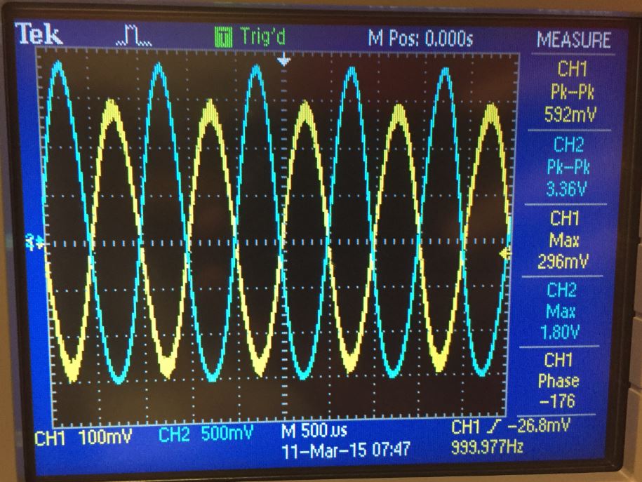
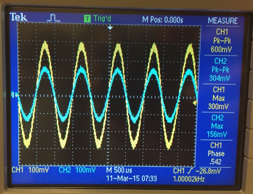
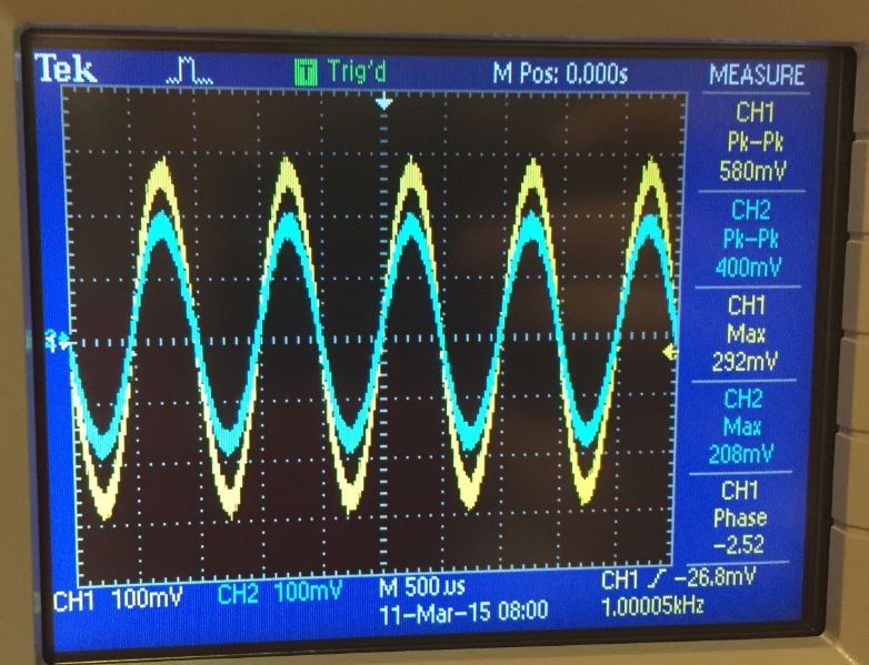
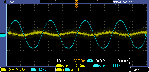
Measuring Gain
To measure the gain of the amplifier circuit, measure the output and
input of the circuit using an oscilloscope probe, find the maximum
value of each and take the output divided by the input. (see below)
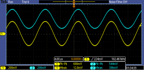
Common drain NMOS gain
Common drain PMOS gain
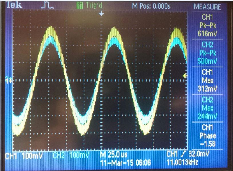
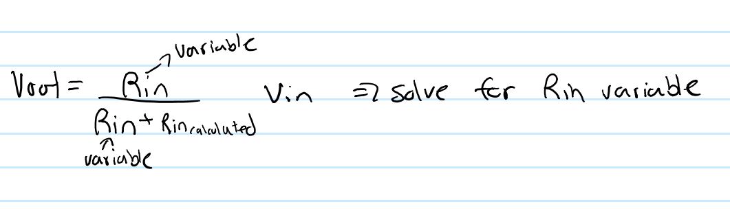
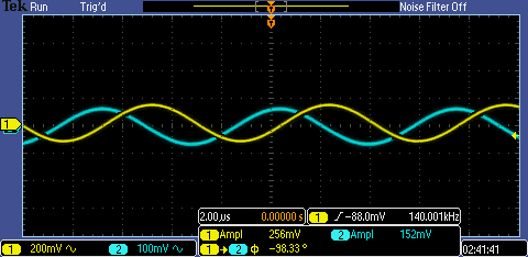
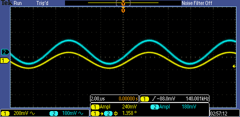
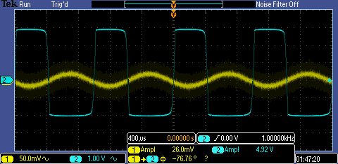
Measuring input/output resistance
Since we cannot measure the input/output resistance of an amplifier
using a multimeter or oscilloscope, we will use a simple voltage
divider. For example to calculate the actual input resistance, we
will ground the output and we will apply an AC signal to a resistor of
the same size as the calculated input resistance in series with a
capacitor to the actual input of the amplifier. Then by measuring the
input and the output, if the value we calculated is exactly the same as
the actual input voltage, we should get half of the signal at the
actual output. (See below) If the value is not the same apply the
voltage divider equation based on the current values of input, output,
and resistance but with Rin as a variable. To calculate the output
resistance, the same process is followed but with the input grounded
and we apply a voltage to the calculated output resistance in series
with a capacitor and the actual amplifier output.
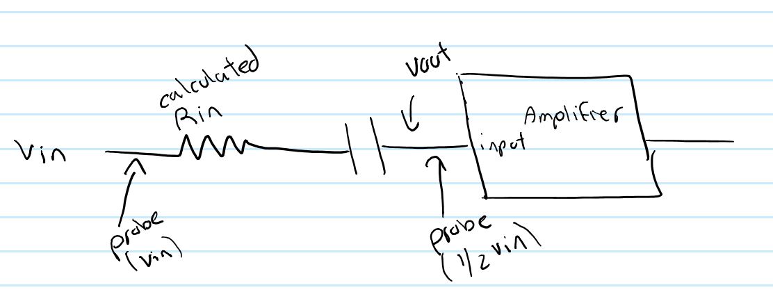
How to measure
voltage divider equation
Below
are the experimental graphs of the input/output resistances of both
NMOS and PMOS CD amplifier. Note that when the output voltage of the
input/output measuring configuration is exactly half of the input, the
voltage divider equation is not needed and the calculated resistance is
the actual resistance. The calculations including the voltage divider
is in the calculations of gain and resistances above when necessary.
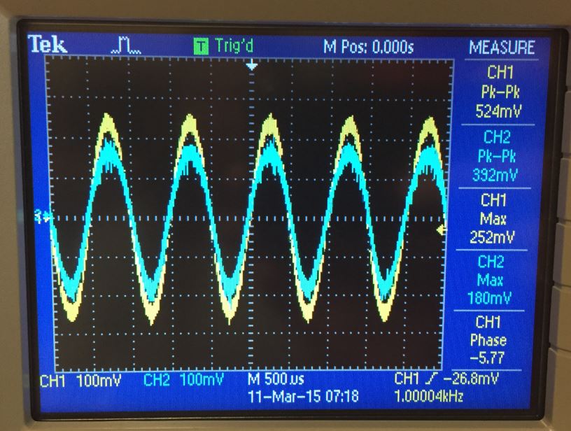
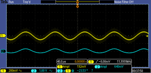
CD NMOS input resistance
CD NMOS output
resistance
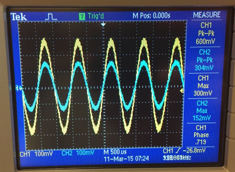
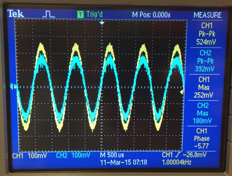
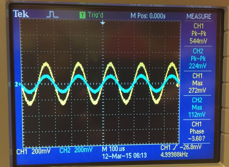
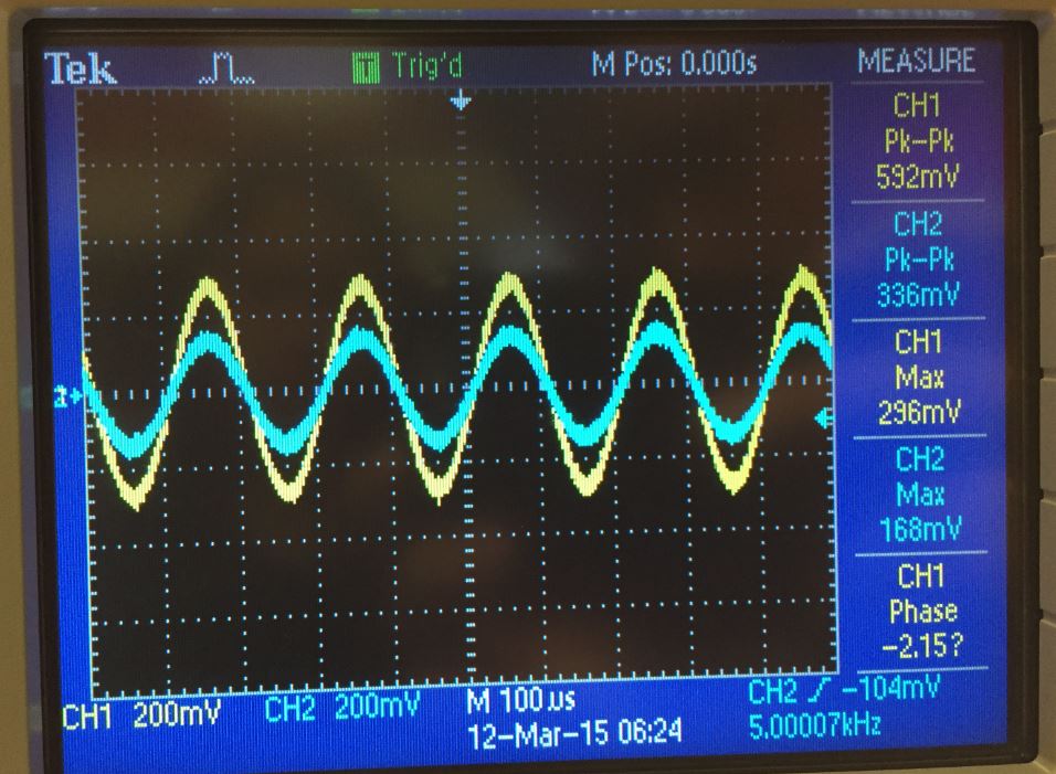
CD PMOS input resistance
CD PMOS output resistance
Simulation results
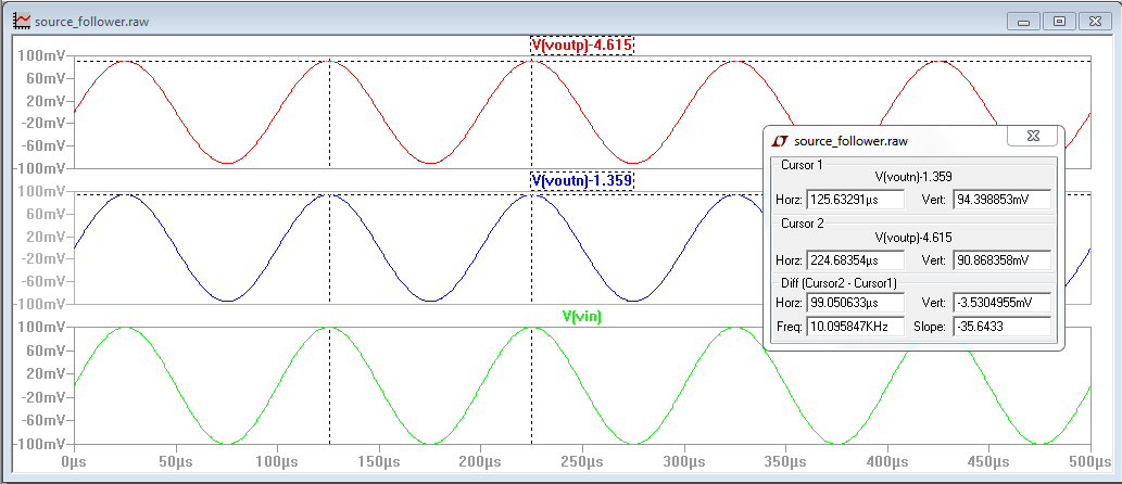
Below is a table of results from calculations, experimental, and simulations
Table of Results:
NMOS
| Hand Calculations | Experimental results | Simulation Results |
| gain | .9524 | .8 | .944 |
| input resistance | 33.33K | 33.33K | N/A |
| output resistance | 47.62 | 273.4 | N/A |
PMOS
| Hand Calculations | Experimental results | Simulation Results |
| gain | .909 | .812 | .909 |
| input resistance | 33.33K | 33.33K | N/A |
| output resistance | 90.91 | 200 | N/A |
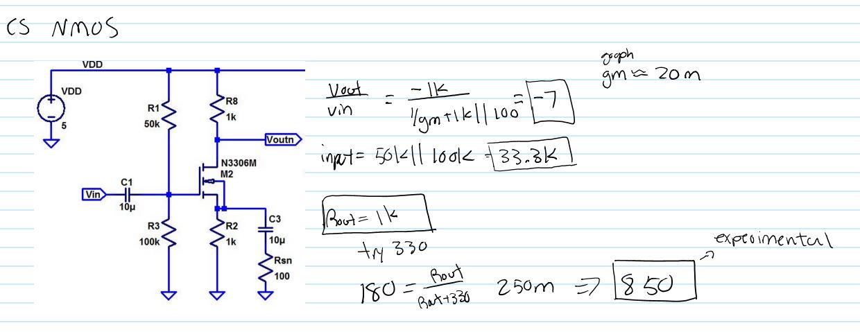
Experiment 2: Common Source Amplifier
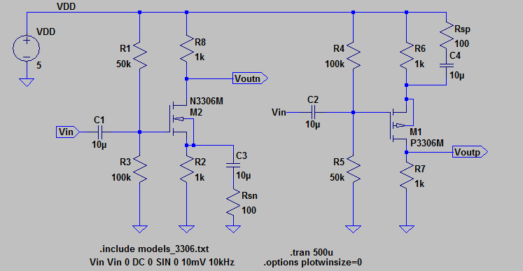
The
hand calculations and experimental simulations of a common source
amplifier are exactly the same the common drain amplifier. The
derivations of gain and input/output resistances are shown below. The
capacitors at the gate are connected the same as in the common drain
(positive to gate input and output to Vin). For the NMOS capacitor at
the source, the positive terminal is at the source input and for the
PMOS capacitor at the source is connected with the positive terminal
connected to the 100 ohm resistor because when looking at DC there is a
lower voltage drop across the smaller resistor therefore, the terminal
of the capacitor connected to the 100 ohm resistor is at a higher
voltage.
Again
there is a DC offset on the output that is caused by the biasing of the
transistor to be in saturation as explained for the CD amplifier.
However, a common source amplifier cannot be used as a level shifter.
NOTE: when looking at the gain equations
of the NMOS AND PMOS common source amplifiers, we can see that Rsn and
Rsp (source resistances) significantly decreases the value of the drain
resistance which leads to a larger gain. From the gain equation, if
Rsn or Rsp were not considered, the denominator of the equation would
go down leading to a larger gain.
Also note that there is a 180 degree phase shift in the circuit.
Hand Calculations
Common source NMOS
Common
source PMOS
Experimental Gain
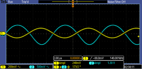
NMOS
gain
PMOS gain
Experimental input/output resistance
NMOS input resistance
NMOS output resistance
NMOS input resistance
PMOS output resistance
Table of results
NMOS
| Hand calculations | Experimental Results | Simulation results |
| gain | -7 | -5.242 | -7 |
| input resistance | 33.33k | 33.33k | N/A |
| output resistance | 1K | 850 | N/A |
PMOS
| Hand calculations | Experimental Results | Simulation results |
| gain | -5.24 | -6.08 | -5 |
| input resistance | 33.33k | 33.33k | N/A |
| output resistance | 1k | 1.159k | N/A |
Experiment 3: Common Gate
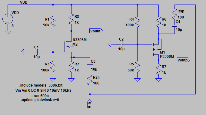
The last basic configuration of amplifiers is the Common Gate
amplifier where the gate is common to the input and output. Similar to
the CS and CD amplifiers, the gain, input/output resistances are
calculated or simulated in a similar. The derivations for these
calculations are shown below. The capacitors for this amplifier is
connected the same as for the CS amplifier.
The
DC offset of the output is caused by the biasing of the amplifier to
ensure it stays in saturation similar to the CD and CS amplifier. Since
the gain is not close to 1, this amplifier cannot be used as a level
shifter.
NOTE:
when looking at the gain equations of the NMOS AND PMOS common source
amplifiers, we can see that Rsn and Rsp (source resistances)
significantly decreases the value of the drain resistance which leads
to a larger gain. From the gain equation, if Rsn or Rsp were not
considered, the denominator of the equation would go down leading to a
larger gain.
Also note that unlike the CS amplifier, this circuit does not have a phase shift.
Hand Calculations
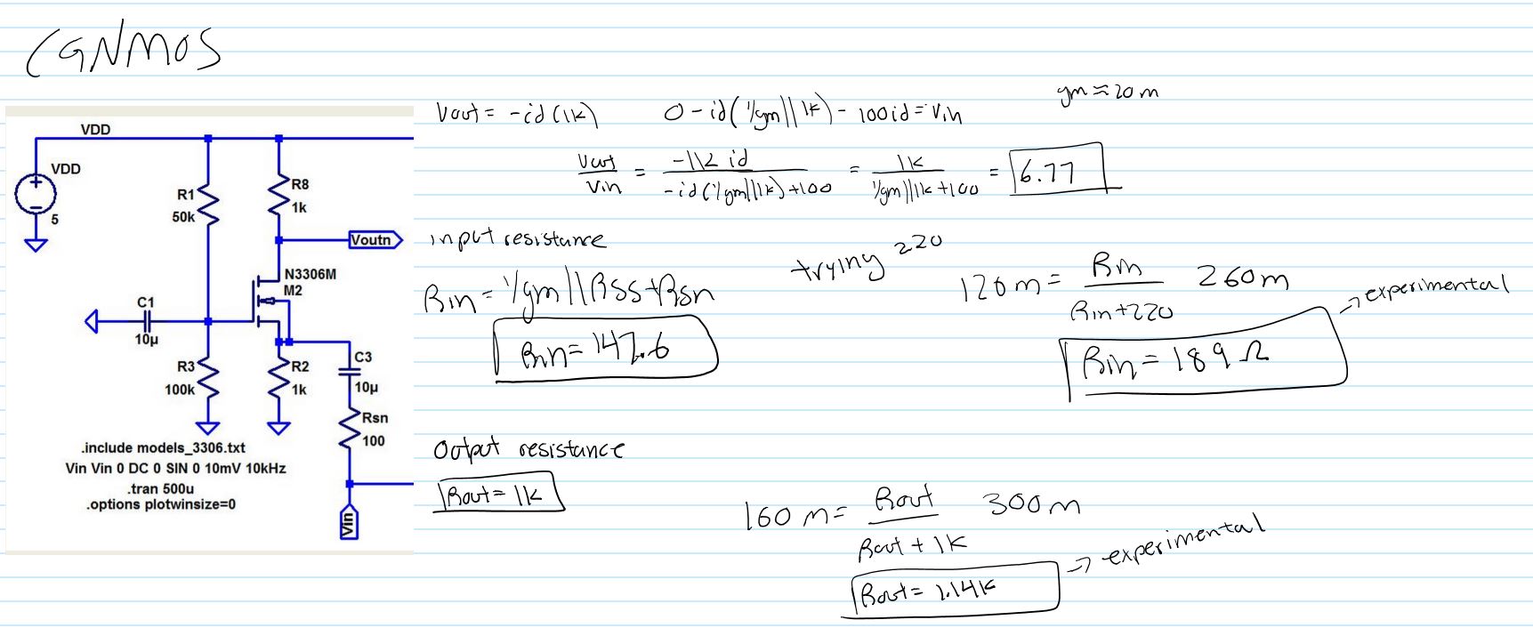
Common Gate NMOS
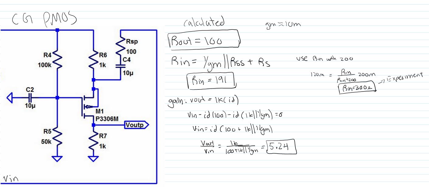
Common Gate PMOS
Experimental Gain
CG NMOS gain
CG PMOS gain
Experimental input/output resistance
CG NMOS input
resistance
CG NMOS output resistance
CG PMOS input
resistance
CG PMOS output resistance
Table of results
NMOS
| Hand calculations | Experimental calculations | Simulation results |
| Gain | 6.77 | .7 | 6.2 |
| input resistance | 147.6 | 189 | N/A |
| output resistance | 1k | 1.159k | N/A |
PMOS
| Hand calculations | Experimental calculations | Simulation results |
| Gain | 5.24 | 3.33 | 4.77 |
| input resistance | 191 | 300 | N/A |
| output resistance | 1k | 1k | N/A |
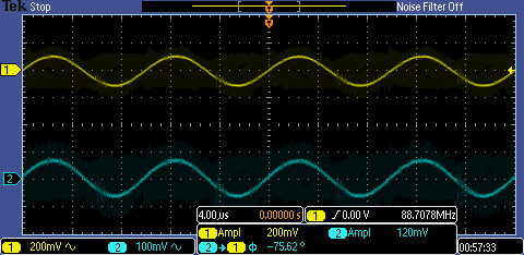
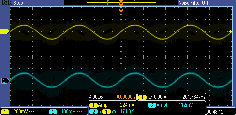
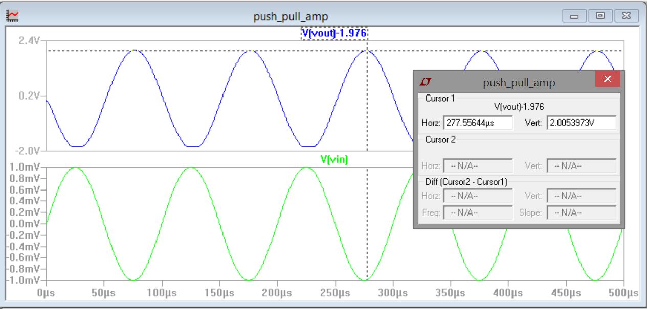
Experiment 4: Push Pull Amplifier
The
last circuit in this lab is a push pull amplifier. The DC operation of
this amplifier will depend on the input offset voltage, if the voltage
is low, the NMOS will turn off and the PMOS will turn on, but if a high
DC voltage is applied, the PMOS will turn off and the NMOS will turn
on. From an AC perspective, we can write our gain equation by relating
the voltage drop across the Rf resistor. (see hand calculations below)
Our hand talcs based on a rough estimate of gmp and gmn gave us a gain
of 3k versus simulations giving a gain of 2K and an experimental gain
of ~1.5K.(simulation results below) The simulation and experimental
results were closer because of the rough estimate of gmn and gmp form
the graph. From our gain formula, we can see that if the resistance of
Rf is increased, the gain will go up proportional to it. This amplifier
is good at sourcing sinking current because it includes both a PMOS and
a NMOS, when the PMOS is on, it sources current and when the NMOS is
on, it will sink current.
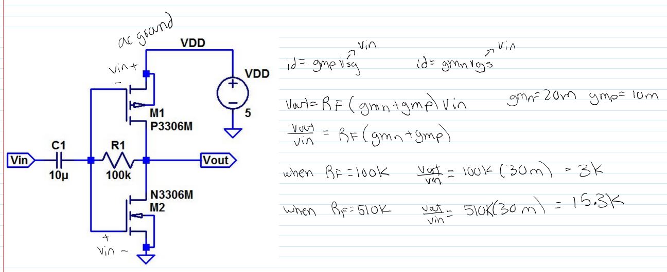
Hand calculations
with 100k Rf
Using 100K
resistor
Using 510K resistor
Add
a return to the listing of your labs