Lab 9 - ECE 420L
Authored
by: Justin Le
Email: lej6@unlv.nevada.edu
April 24, 2015
Goal
Design a beta-multiplier reference (BMR) using the CD4007 CMOS transistor array.
Pre-Lab
Using
the Level=1 MOSFET model created in Lab 8, a BMR was designed that
biases NMOS devices to have a gm of 20 uA/V. A big resistor to VDD
was used as the start-up circuit. The calculations are shown in Figure
0a, and the schematic is shown in Figure 0b. The simulations are shown
in Figures 0c-0d for the output current, NMOS bias voltage, and PMOS
bias voltage as functions of VDD varying from 0 V to 10 V. The LTspice
MOSFET model is shown in Figure 0f.
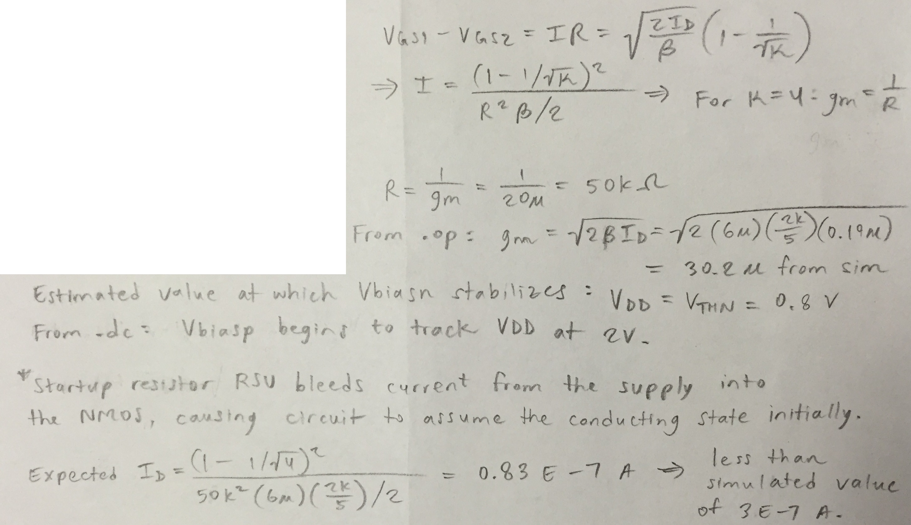
Figure 0a. |

Figure 0b. |
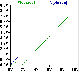
Figure 0c. | 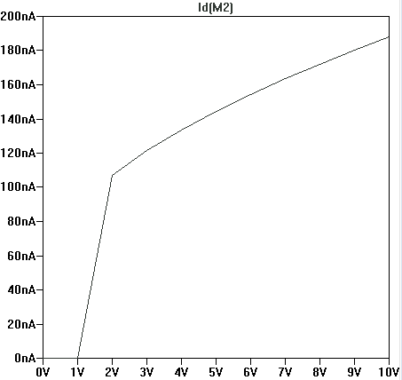
Figure 0d. |
*
*Level=1 models VDD=5V for CD4007
*
.MODEL
N_CD NMOS LEVEL =
1
+ TOX =
1.73E-8 GAMMA = 1
VTO =
1
+ KP = 6E-6
*
.MODEL P_CD PMOS LEVEL =
1
+ TOX =
1.73E-8 GAMMA =
0.33
VTO = -1.5
+ KP = 4.7E-6
*
Figure 0e. |
Experiment 1
The
BMR simulated in the pre-lab was constructed and its output
characterized (Figure 1a-1c). Respectively, the outputs ID, Vbiasp, and
Vbiasn are shown as functions of VDD varying from 0 V to 10 V. After
about 2 V, Vbiasp tracks VDD as the VSG of the PMOS remains constant.
Starting at about 2 V, Vbiasn remains relatively constant in order for
the NMOs to sink the constant current provided by the PMOS above it.
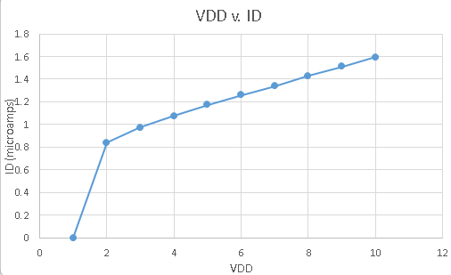
Figure 1a. | 
Figure 1b. | 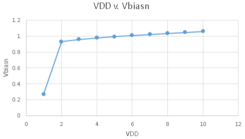
Figure 1c. |
Experiment 2
The
bias voltages generated by the BMR in Experiment 1 were applied to the
gate of a PMOS (Figure 2a) and of an NMOS (Figure 2b) to form a PMOS
and NMOS currentmirror, respectively.

Figure 2a. | 
Figure 2b. |
Experiment 3
The
bias voltages generated by the BMR in Experiment 1 were applied to two
gate-drain-connected PMOS (Figure 3a) and to two
gate-drain-connected NMOS (Figure 3b) to form a PMOS
and NMOS cascode current mirror, respectively.
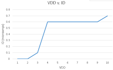
Figure 3a. | 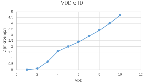
Figure 3b. |
Click to view all labs.