Lab 8 - ECE 420L
Authored
by: Justin Le
Email: lej6@unlv.nevada.edu
April 17, 2015
Goal
Characterize the MOSFETS in the CD4007 transistor array. Model them in LTspice using Level=1 models.
Pre-Lab
Review the datasheet for the CD4007 transistor array and the use of the VSS and VDD pins of the chip.
Experiment 1
For
an NMOS with a VDS held constant at 3 V by a power supply, a plot of ID
versus VGS was generated, for VGS varying from 0 to 3 V (Figure 1a).
The corresponding table of measurements is shown in Figure 1c. The
values for ID were obtained by measuring the output voltage across a
100-ohm resistor and dividing the result by 100. (For all experiments,
the blue channel of the X-Y plot represents the output voltage.)
Similarly,
the VSD of a PMOS was held at 3 V, and a plot of ID versus VSG was
generated, where the values of ID were measured directly by multi-meter
(Figures 1b and 1c).
The simulated curves match the curves generated in the experiment (Figures 1d and 1e).
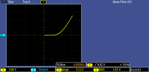
Figure 1a. | 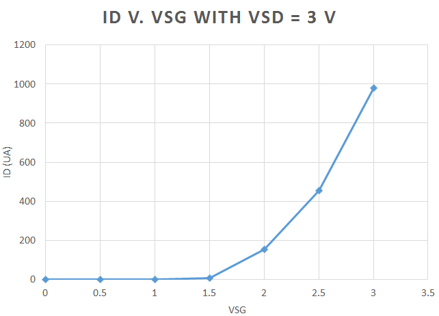
Figure 1b. | 
Figure 1c. |
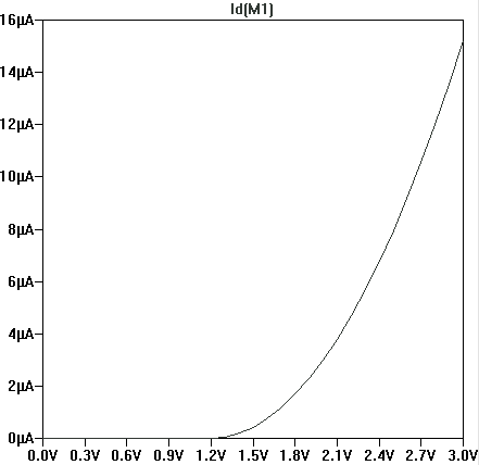
Figure 1d. | 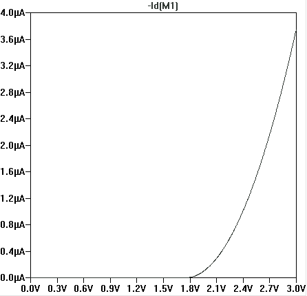
Figure 1e. |
Experiment 2
For
an NMOS, the VGS was held at 1 V, and a plot was generated for ID as
VDS varied from 0 V to 5 V. The measurement was then repeated for each
integer value of VGS from 1 to 5 V. The results are shown respectively
in Figures 2a through 2e.
Figure 2a. | 
Figure 2b. |

Figure 2c. | 
Figure 2d. |
Figure 2e. | |
The
experiment was repeated for a PMOS, with VDS and VGS replaced with VSD
and VSG, respectively, (Figure 2f), and its corresponding measurements
are listed in Figure 2g.
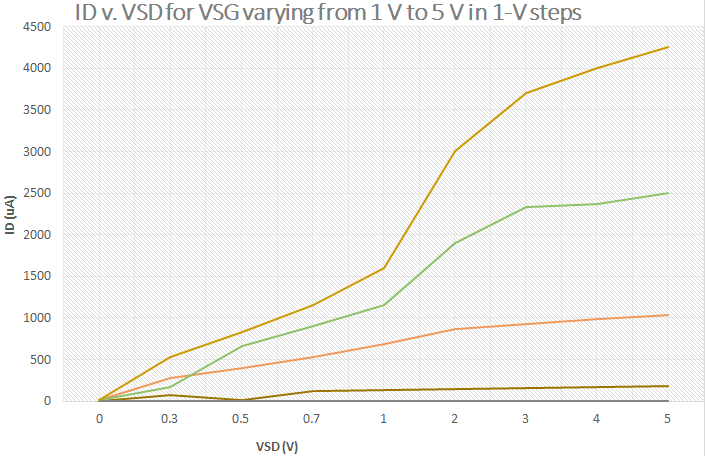
Figure 2f. |
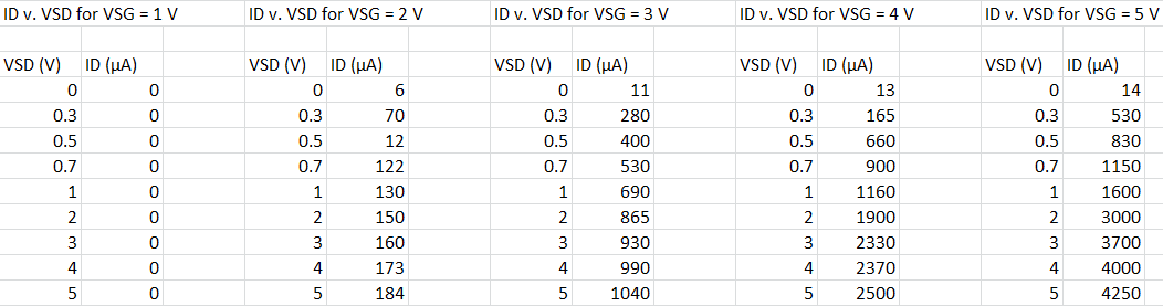
Figure 2g. |
The simulated curves match the curves generated in the experiment (Figures 2h and 2i).
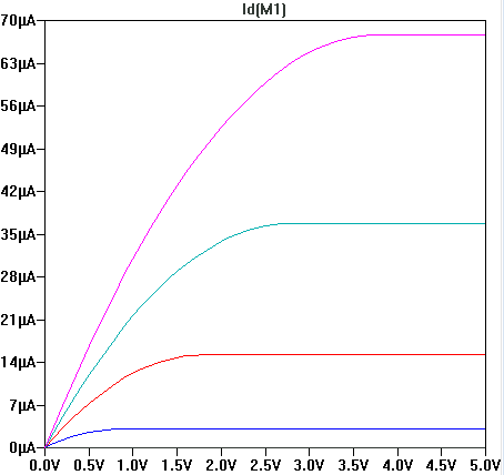
Figure 2h. | 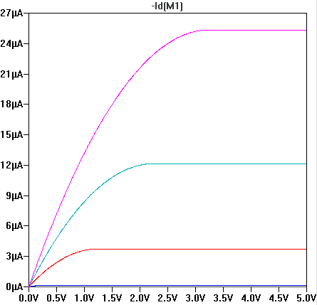
Figure 2i. |
Experiment 3
For
an NMOS with VDS held at 5 V and VSB held at 0 V, a plot was generated
for ID with VGS varying from 0 to 5 V. The measurement was then
repeated for VSB equal to 1, 2, and 3 V. The results are shown
respectively in Figures 3a through 3d.
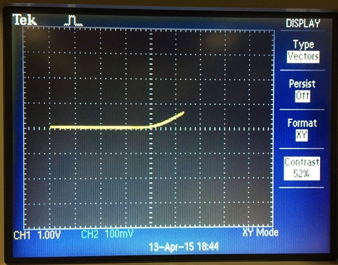
Figure 3a. | 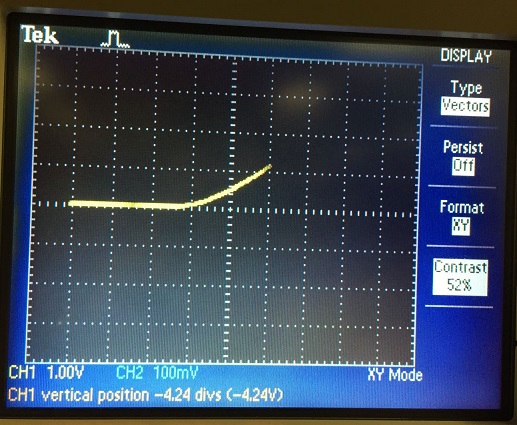
Figure 3b. |
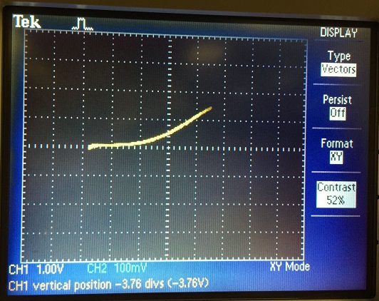
Figure 3c. | 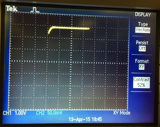
Figure 3d. |
The experiment was repeated for a PMOS, with VDS, VGS, and VSB replaced with VSD, VSG, and VBS, respectively (Figure 3e).
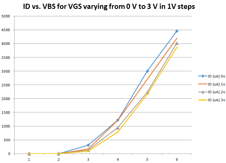
Figure 3e. |
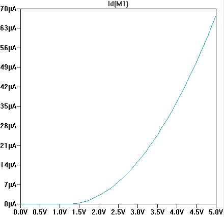
Figure 3f. | 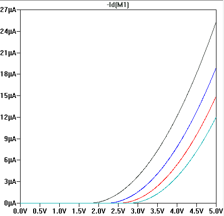
Figure 3g. |
Experiment 4
The
inverting circuit of Figure 4a was built. The time delay of the output
was measured as 50 ns, which matches the value listed in the datasheet
(Figure 4b).
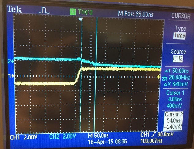
Figure 4b. |
The simulated response of the circuit shows a time delay of 10 μs (Figure 4c), which is not comparable to the 50 ns that was produced experimentally or reported on the datasheet.
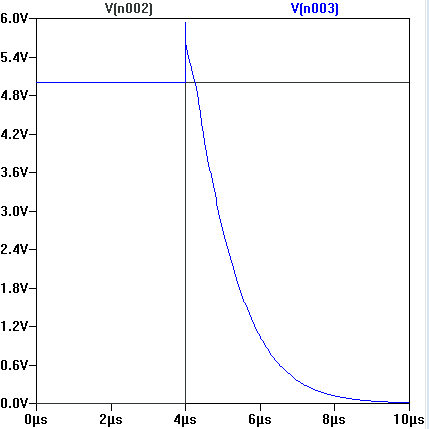
Figure 4c. |
Model
Assuming
that the length of the NMOS is 5 μm and its width is 500 μm, the oxide
thickness is C’ox = Cox/WL = 5pF/(5μm*500μm) = 2 mF. Thus, TOX = ε0*εr/C'ox = 8.85E-12*3.9/2m = 1.73E-8.
KPN = 2ID*L/(W*(VDS,SAT)^2) = (2*300μ*5μ)/(500μ*(2-1)^2) = 6μ.
KPP = 2ID*L/(W*(VSD,SAT)^2) = (2*150μ*5μ)/(500μ*(2-1)^2) = 4.7μ.
By inspection of the plots in Figures 3a and 3b:
GAMMAN = ∆VTH/∆VBS = 1/1 = 1
GAMMAP = ∆VTH/∆VSB = 1/3
By inspection of the plots in Figures 1a and 1b, VOTN = 1 V and VOTP = 1.25 V.
Using only these parameters, a Level = 1 MOSFET model was generated in LTspice (Figure 5a).
*
*Level=1 models VDD=5V for CD4007
*
.MODEL
N_CD NMOS LEVEL =
1
+ TOX =
1.73E-8 GAMMA = 1
VTO =
1
+ KP = 6E-6
*
.MODEL P_CD PMOS LEVEL =
1
+ TOX =
1.73E-8 GAMMA =
0.33
VTO = -1.5
+ KP = 4.7E-6
*
Figure 5 |
Click to view all labs.