Lab 6 - ECE 420L
Authored
by: Justin Le
Email: lej6@unlv.nevada.edu
March 20, 2015
Goal
Demonstrate the operation of single-stage amplifiers using the ZVN3306A and ZVN3306P MOSFETs.
Pre-Lab
Review the video lecture and notes on single-stage amplifiers.
Vary the parameters in the simulation from the lecture to ensure understanding of the circuits.
Experiment 1
The
common-drain amplifiers in Figure 1a were built and their input/output
resistances and gains were measured. The capacitor at the input of each
amplifier is placed with its positive leg facing the gate of the MOSFET
because the gate remains at a higher potential than the voltage source,
which is an AC voltage that varies by only a small amount relative to
the DC voltage caused by VDD.
The input resistance of an
amplifier can be measured by adding a resistor in series with the
voltage source equal to the calculated input resistance. (Additionally,
a capacitor must be added to prevent the DC bias current from being
affected by the added resistor.) The added resistor forms a voltage
divider between itself and the circuit’s input resistance such that the
voltage drop across it is (theoretically) half of the total input
voltage.
Figure 1c shows the calculated resistances and
gains for the two amplifiers. It also shows that by applying the
voltage division equation to the measured input and output voltages of
these amplifiers, an experimental value for the output resistance can
be obtained. The experimental output resistance of the NMOS and PMOS
amplifiers are shown to be 273 Ω and 200 Ω, respectively.
Common-drain
amplifiers are also known as source followers because the output
voltage approximately follows the input voltage, as shown in Figure 1c
where the AC gains are calculated as about 1 and 0.9 The gain can be
estimated as the resistance in the drain (a 1-kΩ resistor) over the
resistance in the source (a 1-kΩ resistor in series with the inverse of
the MOSFET’s transconductance). The NMOS amplifier is biased at
two-thirds the value of VDD, while the PMOS amplifier is biased at
one-third of VDD. The resistor connected to the output is small enough
that the output DC voltage is only about 1 V above ground for the NMOS
amplifier and less than 1 V below VDD for the PMOS amplifier.
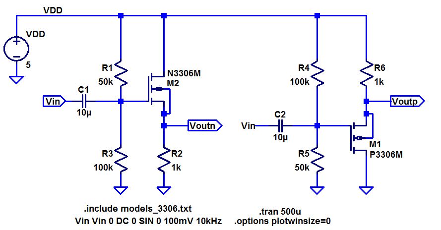
Figure 1a.
| 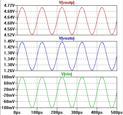
Figure 1b.
|

Figure 1c.
|
Figures
1d and 1e show the voltages when measuring for the NMOS amplifier's
input resistance and output resistance, respectively. Figure 1f shows
the gain.
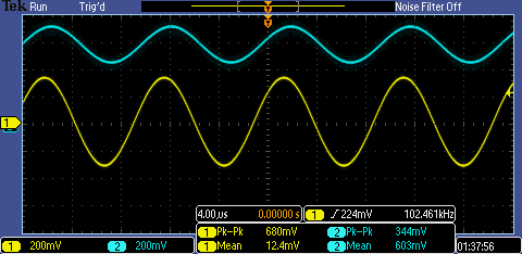
Figure 1d.
| 
Figure 1e.
| 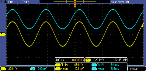
Figure 1f. |
Figures
1g and 1h show the voltages when measuring for the PMOS amplifier's input
resistance and output resistance, respectively. Figure 1i shows the
gain.
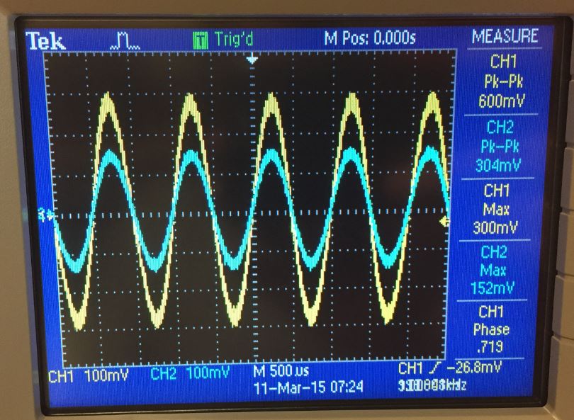
Figure 1g.
| 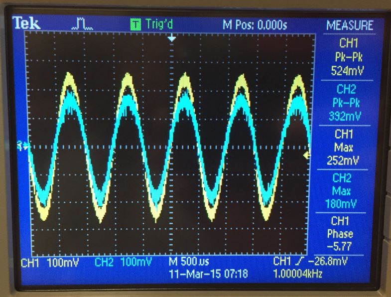
Figure 1h.
| 
Figure 1i. |
Experiment 2
Experiment 1 was repeated for the common-source amplifiers shown in Figure 2a.
Common-source
amplifiers exhibit negative gain, as shown in Figure 2c where the AC
gains are calculated as about –5 and –7. The gain can be estimated as
the resistance in the drain (a 1-kΩ resistor) over the resistance in
the source (the inverse of the MOSFET’s transconductance in series with
the parallel combination of a 1-kΩ resistor and the source resistance).
As in the previous amplifiers, the NMOS amplifier is biased at
two-thirds the value of VDD, while the PMOS amplifier is biased at
one-third of VDD. This bias voltage, along with a 1-kΩ resistor in the
source of each MOSFET, causes the output DC voltage to be 3.6 V and 0.4
V for the NMOS and PMOS amplifiers, respectively.
As
shown by the calculation in Figure 2c, a greater source resistance
would increase the amplifier’s gain in the positive direction, bringing
it closer to zero.
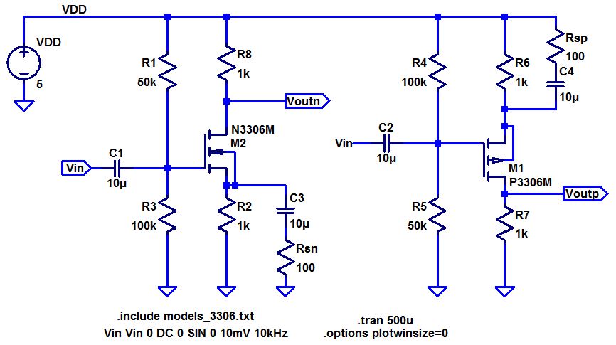
Figure 2a.
| 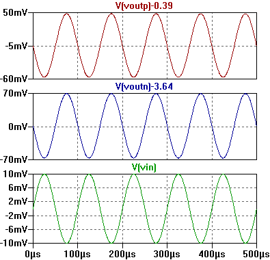
Figure 2b.
|
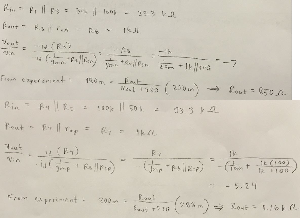
Figure 2c.
|
Figures 2d and 2e show the voltages when measuring for the NMOS amplifier's
input resistance and output resistance, respectively. Figure 2f shows
the gain.
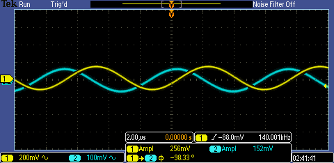
Figure 2d.
| 
Figure 2e.
| 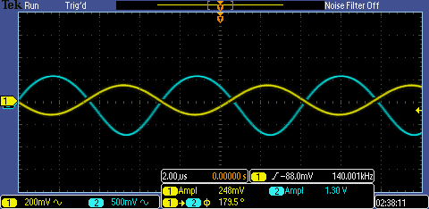
Figure 2f. |
Figures 2g and 2h show the voltages when measuring for the PMOS amplifier's input
resistance and output resistance, respectively. Figure 2i shows the
gain.

Figure 2g.
| 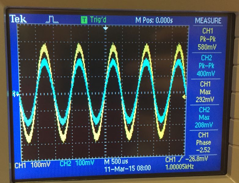
Figure 2h.
| 
Figure 2i. |
Experiment 3
Experiment 1 was repeated for the common-gate amplifiers shown in Figure 3a.
Common-gate
amplifiers exhibit positive gain, as shown in Figure 3c where the AC
gains are calculated as about 7 and 5. The gain can be estimated as the
resistance in the drain (a 1-kΩ resistor) over the resistance in the
source (the inverse of the MOSFET’s transconductance in series with the
parallel combination of a 1-kΩ resistor and the source resistance). As
in the previous amplifiers, the NMOS amplifier is biased at two-thirds
the value of VDD, while the PMOS amplifier is biased at one-third of
VDD. As in the common-source amplifiers, the bias voltage, along with a
1-kΩ resistor in the source of each MOSFET, causes the output DC
voltage to be 3.6 V and 0.4 V for the NMOS and PMOS amplifiers,
respectively.
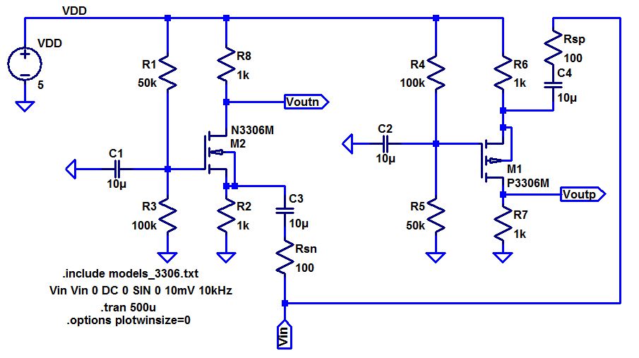
Figure 3a.
| 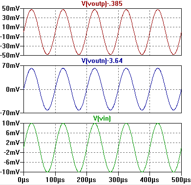
Figure 3b.
|
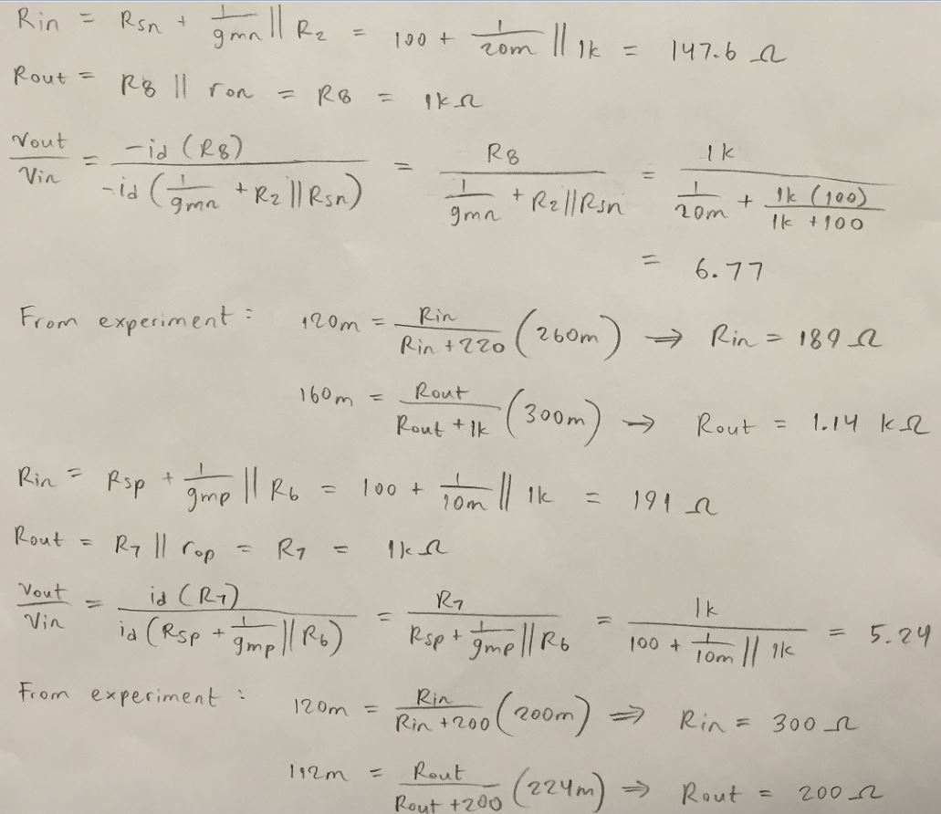
Figure 3c.
|
Figures 3d and 3e show the voltages when measuring for the NMOS amplifier's
input resistance and output resistance, respectively. Figure 3f shows
the gain.
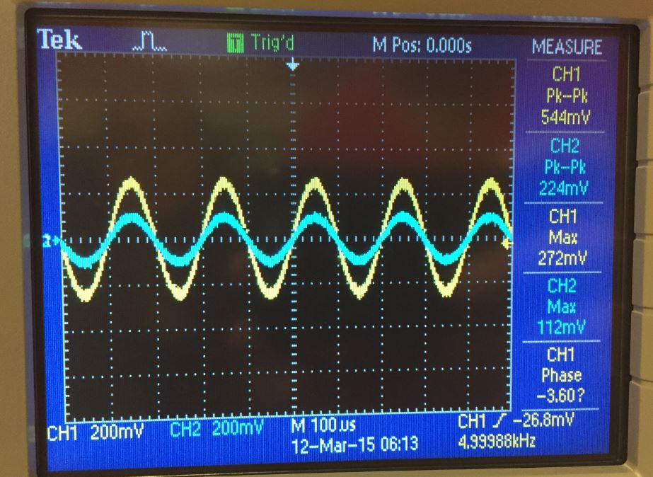
Figure 3d.
| 
Figure 3e.
| 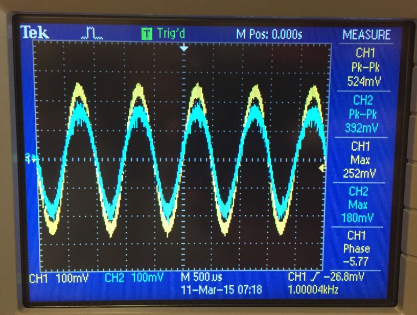
Figure 3f. |
Figures 3g and 3h show the voltages when measuring for the PMOS amplifier's input
resistance and output resistance, respectively. Figure 3i shows the
gain.

Figure 3g.
| 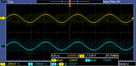
Figure 3h.
| 
Figure 3i. |
Experiment 4
The
push-pull amplifier in Figure 4a built, and its gain was measured. This
amplifier is good at both sinking and sourcing current: when the offset
of the source voltage is low, the PMOS conducts and the amplifier
sources current, and when the offset is high, the NMOS conducts and the
amplifier sinks current. As shown in Figure 4c, the AC gain is directly
dependent on the transconductances of the MOSFETs and on the resistor.
When a 510-kΩ resistor is used, the gain is 15.3k, which is greater
than the gain of 3k that results when a 100-kΩ resistor is used. That
is, a larger resistor causes a larger gain in the push-pull amplifier.
The relationship between output and input voltage is written by
equating the current through the resistor with the currents that pass
through each MOSFET.
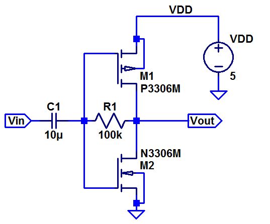
Figure 4a.
| 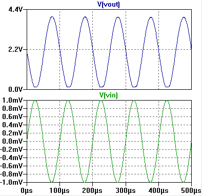
Figure 4b.
|
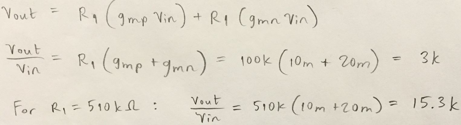
Figure 4c.
|
Figures 4d and 4e show the gain when using a 100-kΩ and 510-kΩ resistor, respectively.
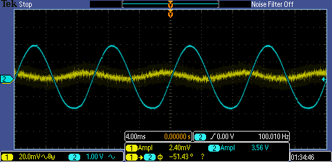
Figure 4d.
| 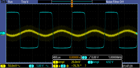
Figure 4e.
|
Figures
For Experiment 1:
a: Schematic.
b: Simulation.
c: Calculations.
d–i: Measurements.
For Experiment 2:
a: Schematic.
b: Simulation.
c: Calculations.
d–i: Measurements.
For Experiment 3:
a: Schematic.
b: Simulation.
c: Calculations.
d–i: Measurements.
For Experiment 4:
a: Schematic.
b: Simulation.
c: Calculations.
de: Measurements.
Click to view all labs.