Lab 5 - ECE 420L
Authored
by: Justin Le
Email: lej6@unlv.nevada.edu
March 6, 2015
Goal
Demonstrate the frequency response of a triangle wave generation circuit that uses the LM324 op-amp.
Pre-Lab
Review the third video lecture and notes on op-amps.
Vary the parameters in the simulation from the lecture to ensure understanding of the circuit.
Experiment 1
The circuit shown in Figure 1a was built and tested using VCC+ = 5 V and VCC- = 0 V.
The 100-kΩ resistor in the feedback
loop can be neglected to simplify the calculation because it is large enough
that its parallel combination with the capacitor will approximate the
capacitor’s impedance. The resulting frequency response is calculated in Figure
1b.
The circuit does not work without the
100-kΩ resistor because it provides a path for the DC current to flow from
output to input. Without the resistor, the feedback loop would act as an open
circuit at low frequencies.
The 100-kΩ resistor has no effect on
the frequency response because the capacitor acts as an AC short, effectively
removing the resistor from the circuit.
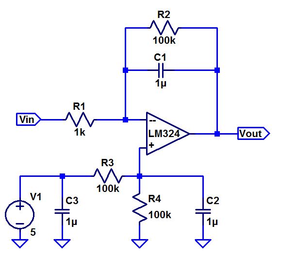
Figure 1a.
| 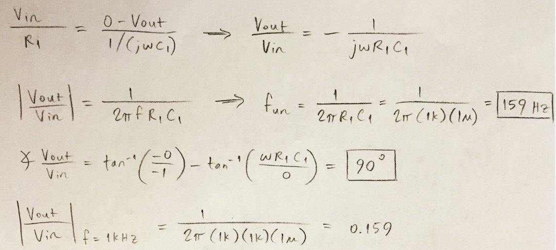
Figure 1b.
|
Figure 1c shows that the gain is about
one-fifth as calculated in Figure 1b for a frequency of 1 kHz. (The oscilloscope
measures a peak-to-peak output that is greater than one-fifth of the input due
to the spikes that occur at each half-period interval.) Figure 1d shows that
the gain is at unity for a frequency of 160 Hz, as calculated. (Again, the
regular spikes in output voltage cause the scope to measure a greater
peak-to-peak voltage.)
The phase-shift does not match the calculated
value because as the frequency increases, the capacitor draws more current away
from the resistor, causing the resistance to be effectively zero and the second
term in the phase calculation to be zero. Thus, the phase-shift approaches 180 –
0 = 180 degrees as the frequency increases beyond the unity-gain frequency.
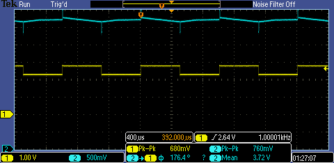
Figure 1c.
| 
Figure 1d.
|
Experiment 2
The
topology shown in Figure 1a was used
to design a triangle wave generation circuit that would operate at 10
kHz with
a an output voltage that swings from 1 to 4 V centered around 2.5 V and
would take
a square wave as an input. Based on the calculation shown in Figure 2a,
the input
resistance was chosen to be 10 kΩ for a feedback capacitance of 0.33 nF
and an input voltage swing of 0.2 V. The measured waveforms are shown
in Figure 2b.
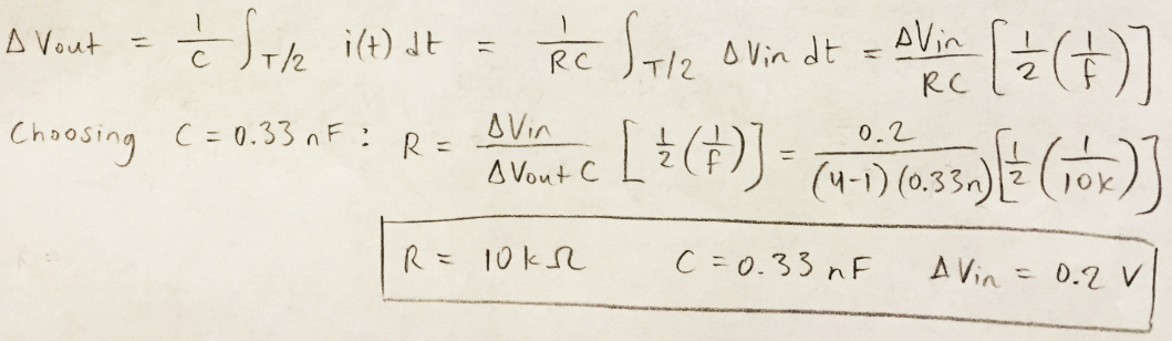
Figure 2a.
| 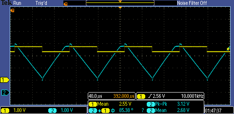
Figure 2b.
|
Figures
For Experiment 1:
a: Schematic.
b: Calculation.
cd: Measurements.
For Experiment 2:
a: Calculation.
b: Measurement.
Click to view all labs.