Lab 2 - ECE 420L
Authored
by: Justin Le
February 20, 2015
Email: lej6@unlv.nevada.edu
Goal
Use basic op-amp configurations to measure the gains and offsets of the LM324 op-amp.
Pre-Lab
Review the first lecture on op-amps and simulate the circuit in Figure 2a.
Discussion
As
shown in the Figure 1a, the minimum common-mode voltage (VCM) of the
LM324 at an ambient temperature of 25 degrees Celsius is 0 V and the
maximum is VCC – 1.5, which is 5 – 1.5 = 3.5 V for this experiment.
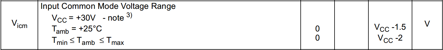
Figure 1a.
|
The
LM324’s open-loop gain can be estimated as 100 dB or 100k by inspecting
Figure 1b for the value corresponding to a power supply voltage of 5 V.
In Figure 1c, a similar open-loop gain can be obtained for frequencies
near 10 Hz, and also, in Figure 1d, the average open-loop gain is
listed as 100 dB.
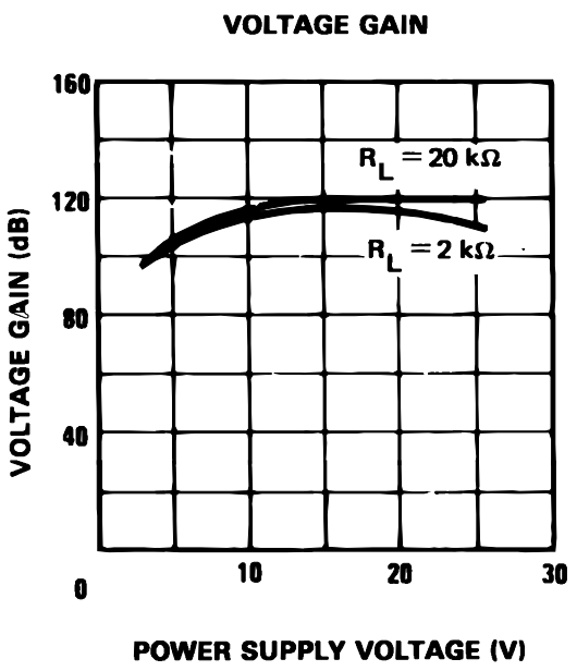
Figure 1b.
| 
Figure 1c.
|
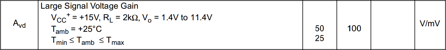
Figure 1d.
|
The input offset voltage can be estimated as 2 mV, as listed in Figure 1e for an ambient temperature of 25 degrees Celsius.
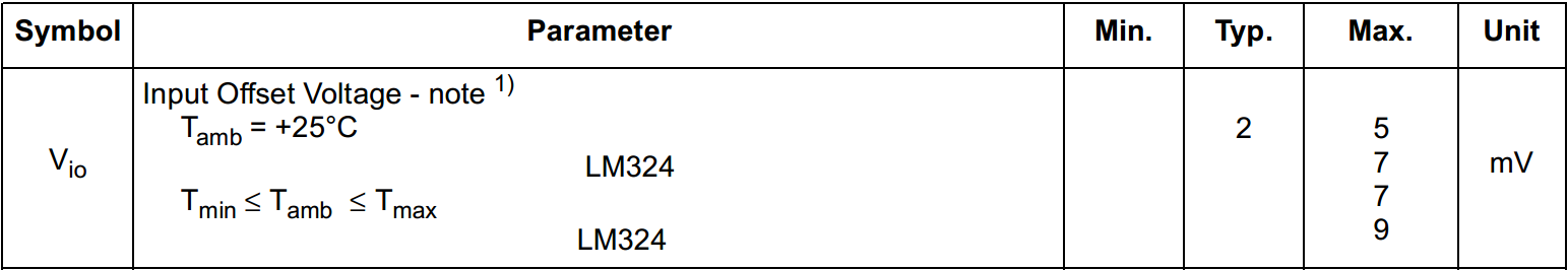
Figure 1e.
|
Experiment 1
The
circuit in Figure 2a was built and tested using the LM324. The
following seven points describe the characteristics and operation of
the circuit.
Figure 2a.
|
1.
The 5-V source and voltage divider at the op-amp’s input causes the common-mode voltage (VCM) to remain fixed at 2.5 V.
2.
The ideal closed-loop gain is
– Rf / Ri = – 5k / 5k = – 1.
3.
The
output swing is centered around VCM = 2.5 V because VCM is equal to the
DC input voltage, causing the potential difference across the input
resistor to be zero and the current through the resistor to also be
zero. As no current flows through the input resistor and negligible
current flows into the op-amp’s negative input terminal, a negligible
current flows in the feedback loop of the circuit, and consequently,
the DC output voltage approximates the input voltage. Figure 3a shows
the AC input and output voltages, and Figure 3b shows the complete
signals centered around 2.5 V.
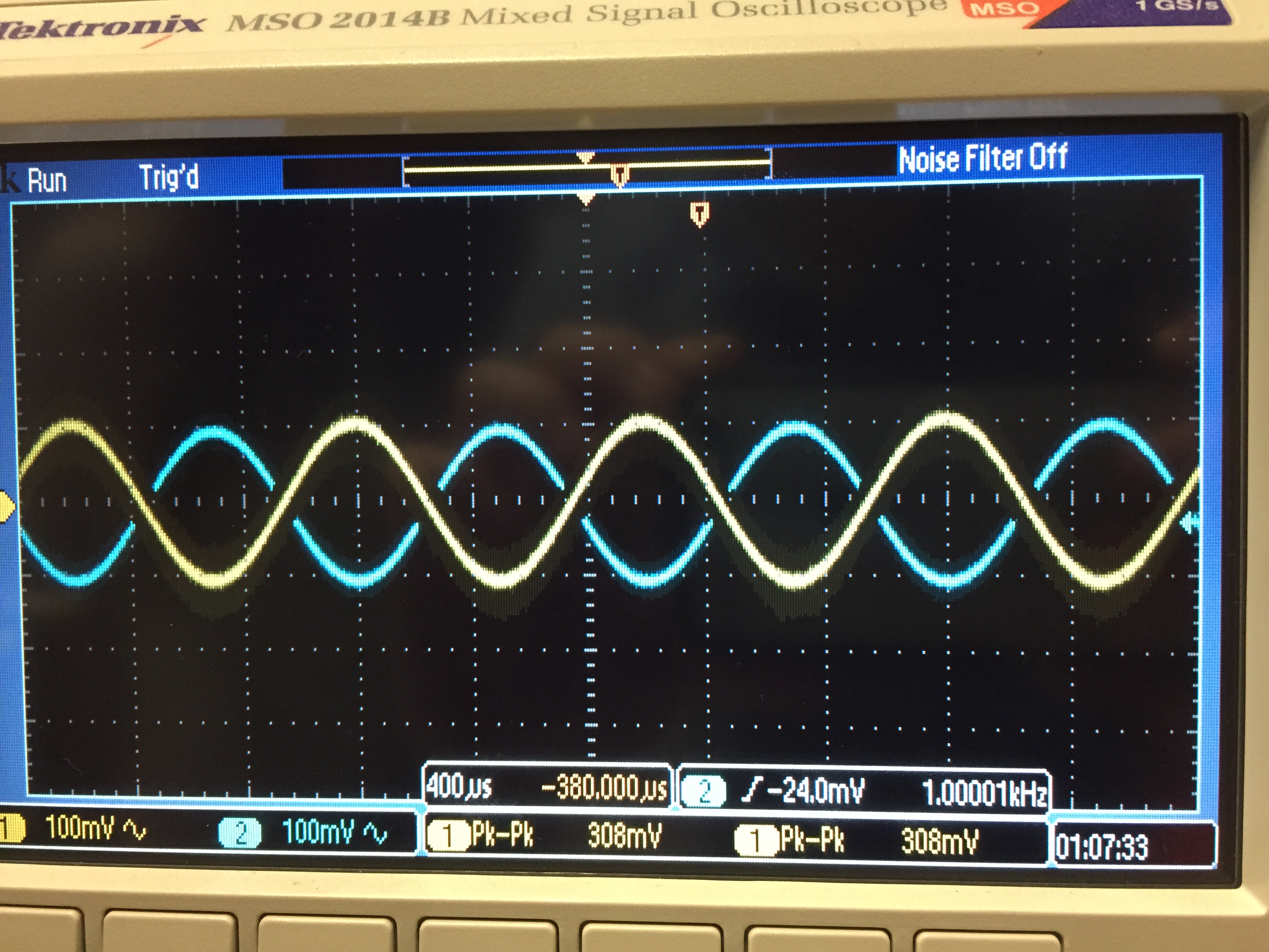
Figure 3a.
| 
Figure 3b.
|
If
VCM is less than 2.5 V, the output may saturate at lower voltages due
to the maximum swing allowed by the supply voltage. Specifically, if
the output is centered around a voltage that is approximately one
amplitude above the lower supply voltage (0 V), then the troughs of the
output signal begin to clip.
Similarly, the crests of the
output signal begin to clip when the signal is centered around a
voltage that is nearly one amplitude below the higher supply voltage (5
V).
4.
At a gain of 1, the maximum allowable
input signal amplitude is 2.5 V. At this amplitude, the output signal
has a peak voltage of 2.5 (DC level) + 2.5 (AC amplitude) = 5 V, which
equals the supply voltage, or the voltage at which the signal begins to
saturate. Figures 3c and 3d show that even a 1.9-V amplitude is
sufficient to cause saturation.
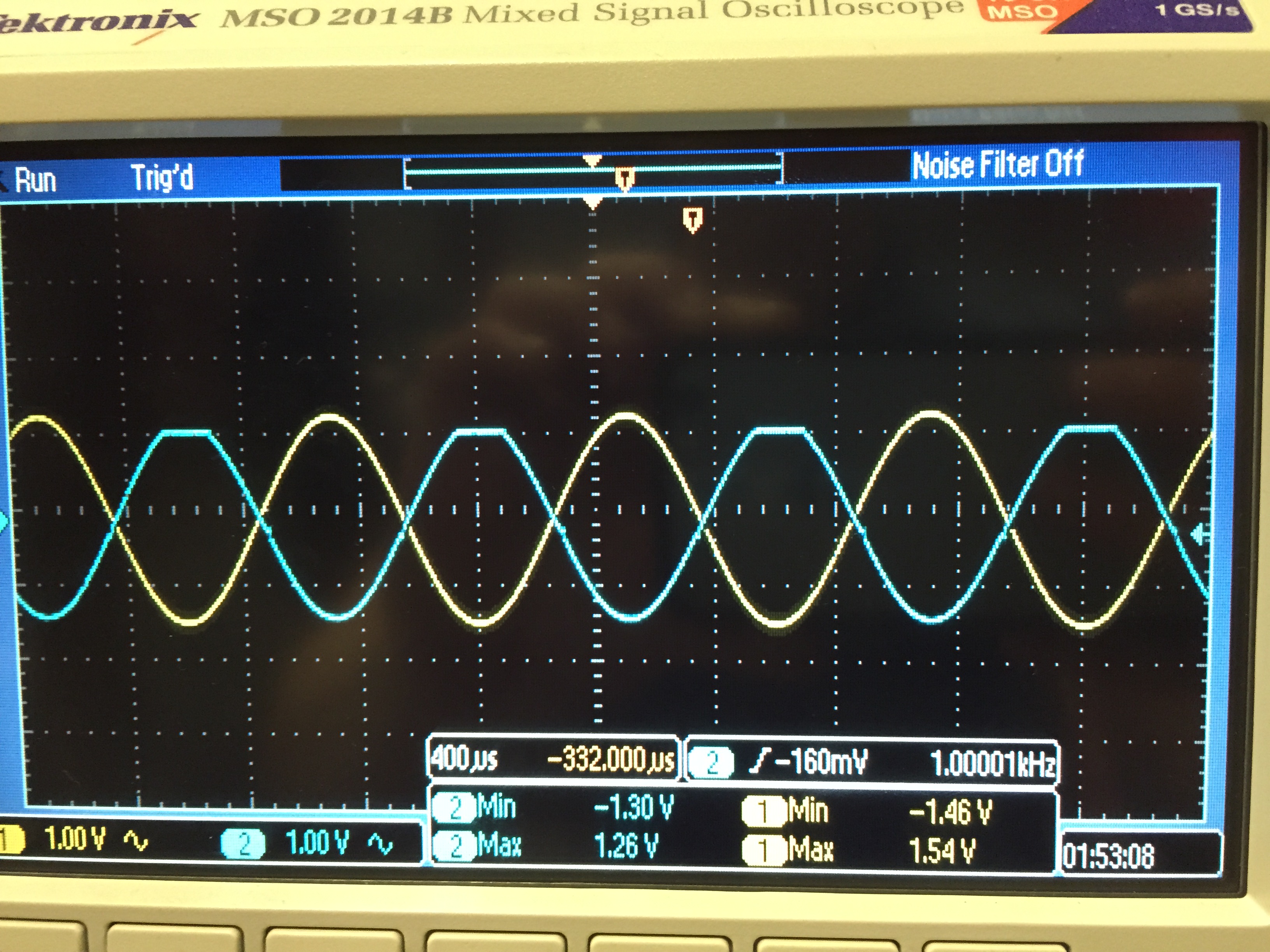
Figure 3c.
| 
Figure 3d.
|
5.
At
a gain of 10, the maximum allowable input signal amplitude is 250 mV,
which causes the output signal amplitude to be 250m x 10 = 2.5 V. The
output signal amplitude then has a peak of 2.5 (DC level) + 2.5 (AC
amplitude) = 5 V, which equals the supply voltage, or the voltage at
which the signal begins to saturate. Figures 3e and 3f show that a
210-mV input signal amplitude is sufficient to cause saturation.
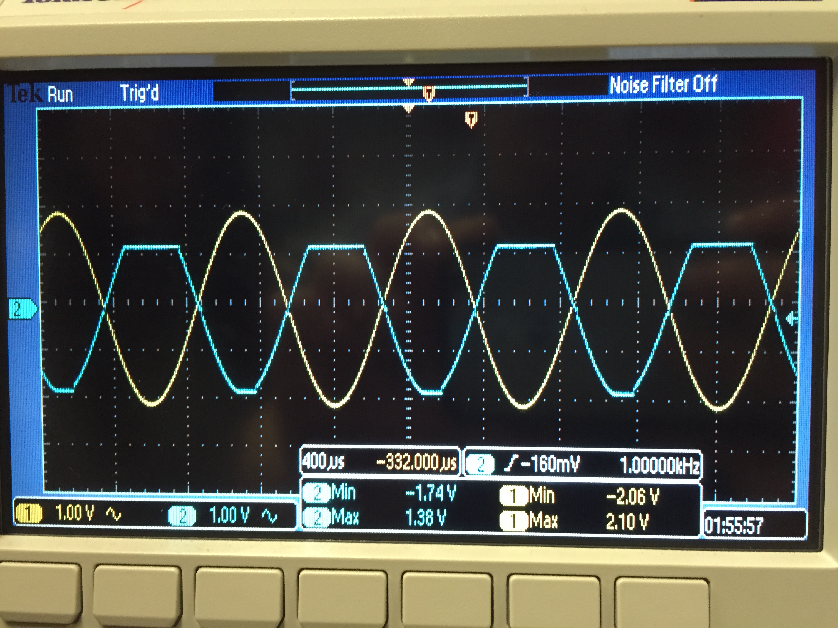
Figure 3e.
| 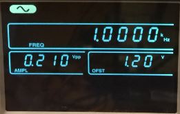
Figure 3f.
|
6.
Changes
in the supply voltage due to noise are smoothed by the capacitors. The
voltage across the capacitor cannot change instantly, and the capacitor
acts as an AC short. Thus, the abrupt and unpredictable high-frequency
fluctuations caused by noise are not seen at a node where a grounded
capacitor is tied. The values of these capacitors are not critical
because any small capacitance is sufficient to provide a time-constant
small enough for it to charge and discharge promptly.
7.
In
order to estimate the effect of the input resistors on the input bias
current, the voltage source can be treated as a short circuit, in which
case, the resistors are in parallel. For relatively small resistors,
such as 10 kΩ, the voltage due to the 20 nA input bias current is
small: 20n * (10k || 10k) = 100 µV. For larger resistors, such as 100
MΩ, the voltage due to the input bias current increases to 20n * (100M
|| 100M) = 1 V. The voltage at the op-amp’s input is effectively 2.5
(input source) + 1 (input bias voltage) = 3.5 V, which creates a
significant potential difference across the input resistor and allows
much greater current to flow in the circuit than the initial 10 kΩ
resistors allowed. The result is an output voltage high enough to
saturate significantly.
The input offset current is the
difference between the input bias current at the positive and negative
inputs of the op-amp, respectively. For the LM324, it is listed on the
datasheet as 2 nA, but for the purpose of these experiments and
calculations, it is estimated to be zero.
Experiment 2
In
the circuit shown in Figure 4a, the offset voltage can be estimated by
measuring the potential difference between the output voltage and the
positive input terminal of the op-amp and dividing the measured value
by the closed-loop gain of 20k / 1k = 20. This difference is expected
to be zero because no current flows in the circuit and the output
voltage is expected to equal VCM (see point 3 in Experiment 1). Any
difference between output and VCM, then, is the consequence of input
offset voltage.

Figure 4a.
|
For
smaller input offset voltages, selecting RF = 100k increases the gain
to 100k / 1k = 100, which amplifies the difference to an amount great
enough to be measured.
Figures 5a through 5d show the
measured values for four different LM324 op-amps with a closed-loop
gain of 100, which are 36.2 mV, 49.6 mV, 104.3 mV, and 38.4 mV,
respectively. From these measurements, the input offset voltages are
estimated as 0.36 mV, 0.5 mV, 1.04 mV, and 0.38 mV, respectively.
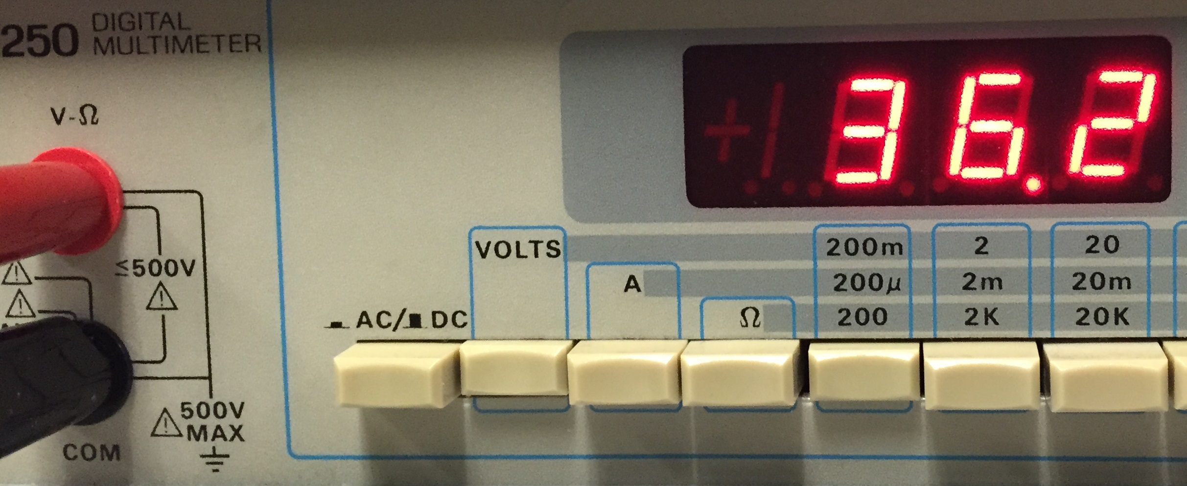
Figure 5a.
| 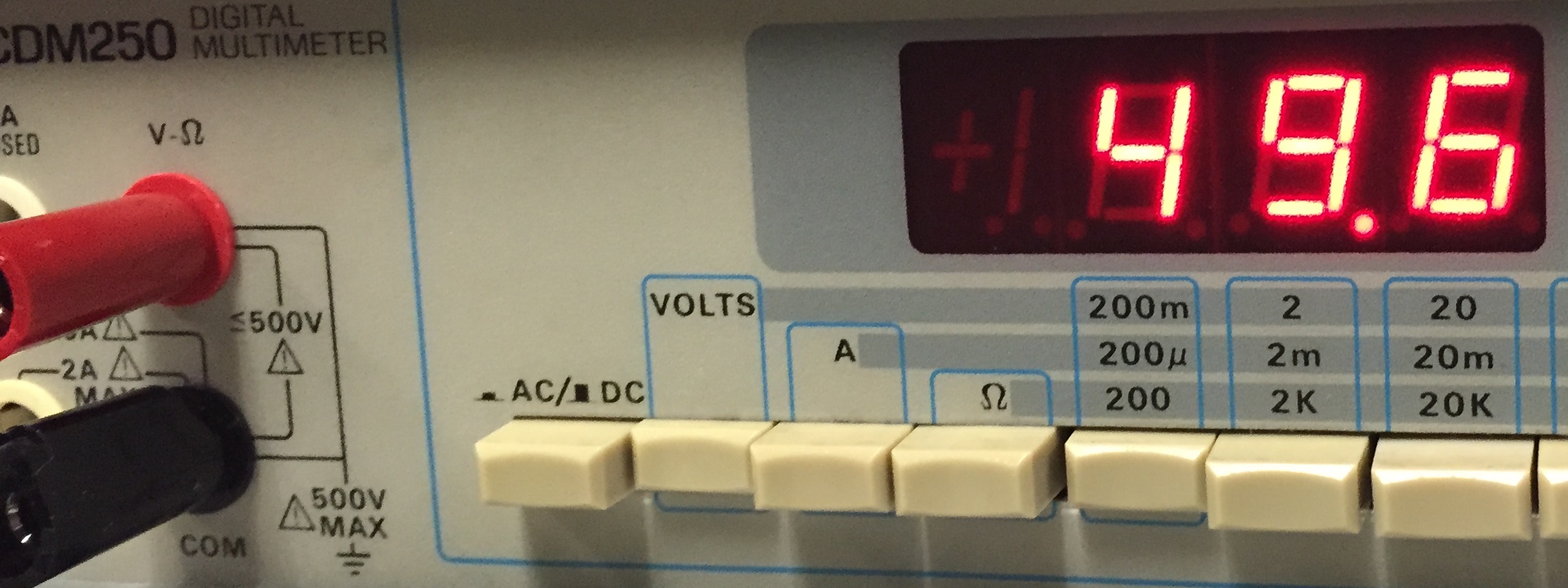
Figure 5b.
|
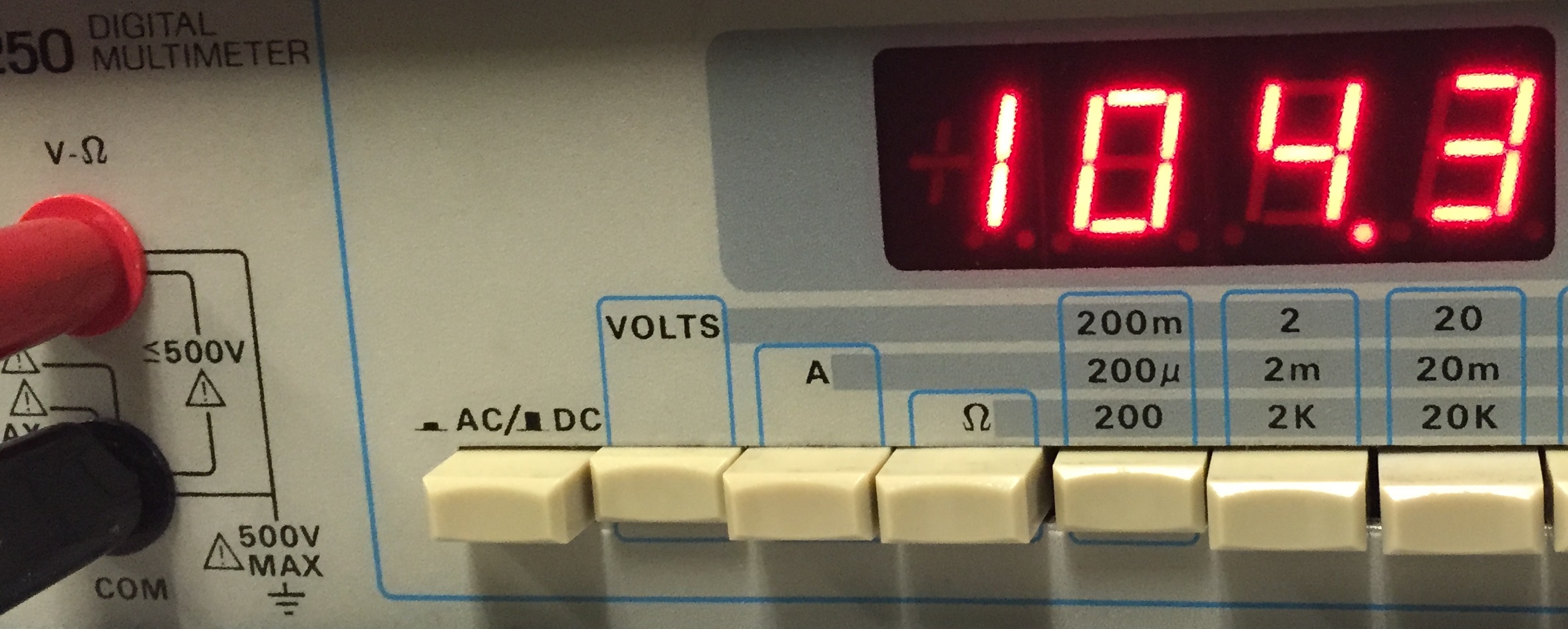
Figure 5c.
| 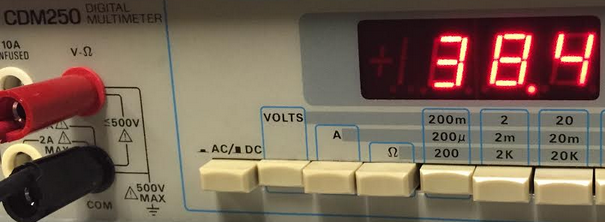
Figure 5d.
|
Figures
For Discussion:
a-d: Datasheet values.
For Experiment 1:
2a: Schematic.
3a-f: Laboratory results.
For Experiment 2:
4a: Schematic.
5a-d: Laboratory results.
Click to view all labs.