Lab 2 - ECE 420L
Authored
by: Justin Le
February 6, 2015
Email: lej6@unlv.nevada.edu
Pre-Lab
Review the video lecture and notes on scope probes.
Vary the parameters in the simulation from the lecture to ensure understanding of the circuit.
Review the operation and analysis of simple RC circuits and Bode plots.
Experiment 1
Shown in order are waveforms measured by a 10:1 probe undercompensated, overcompensated, and compensated correctly.
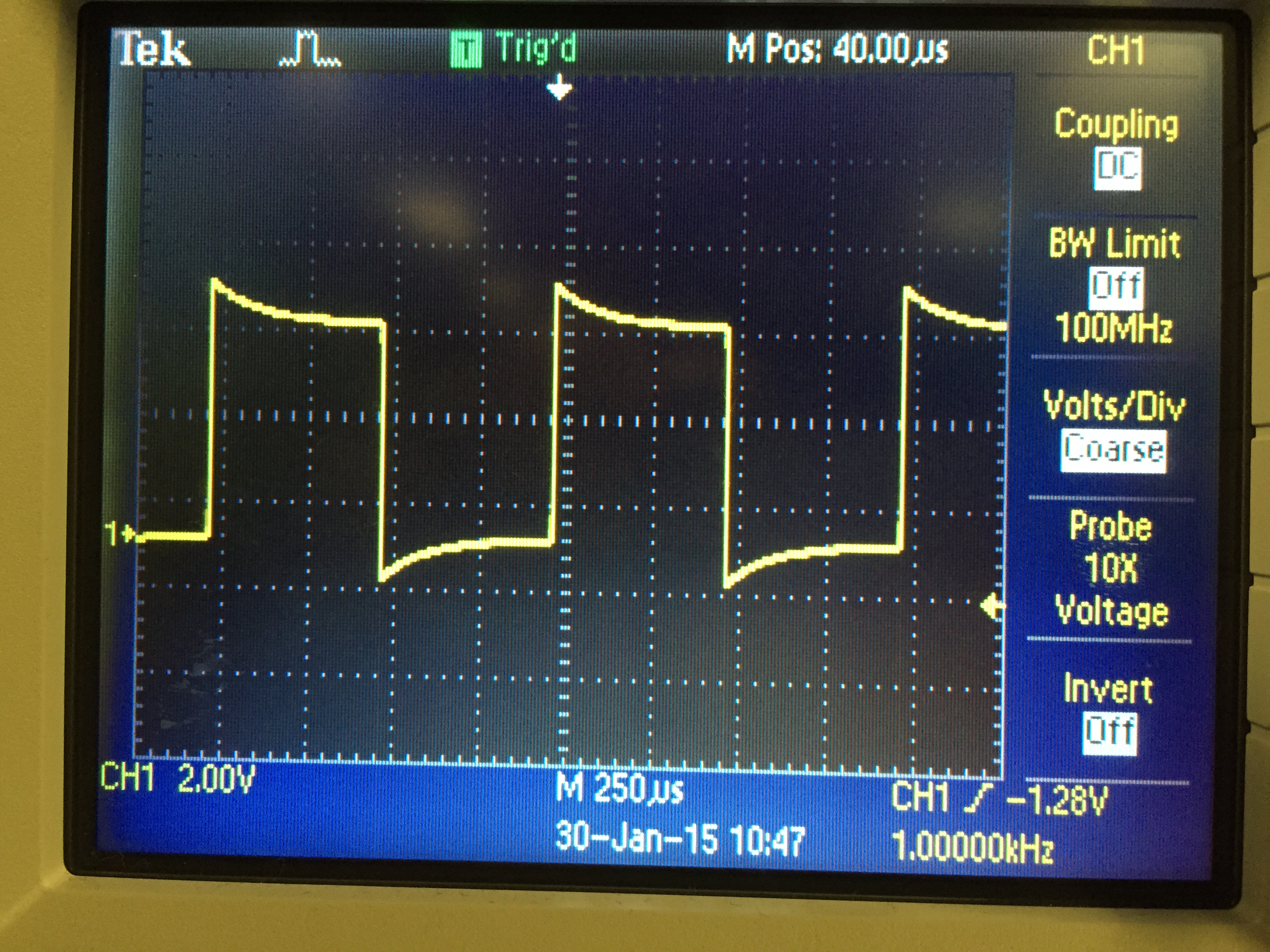
Figure 1a.
| 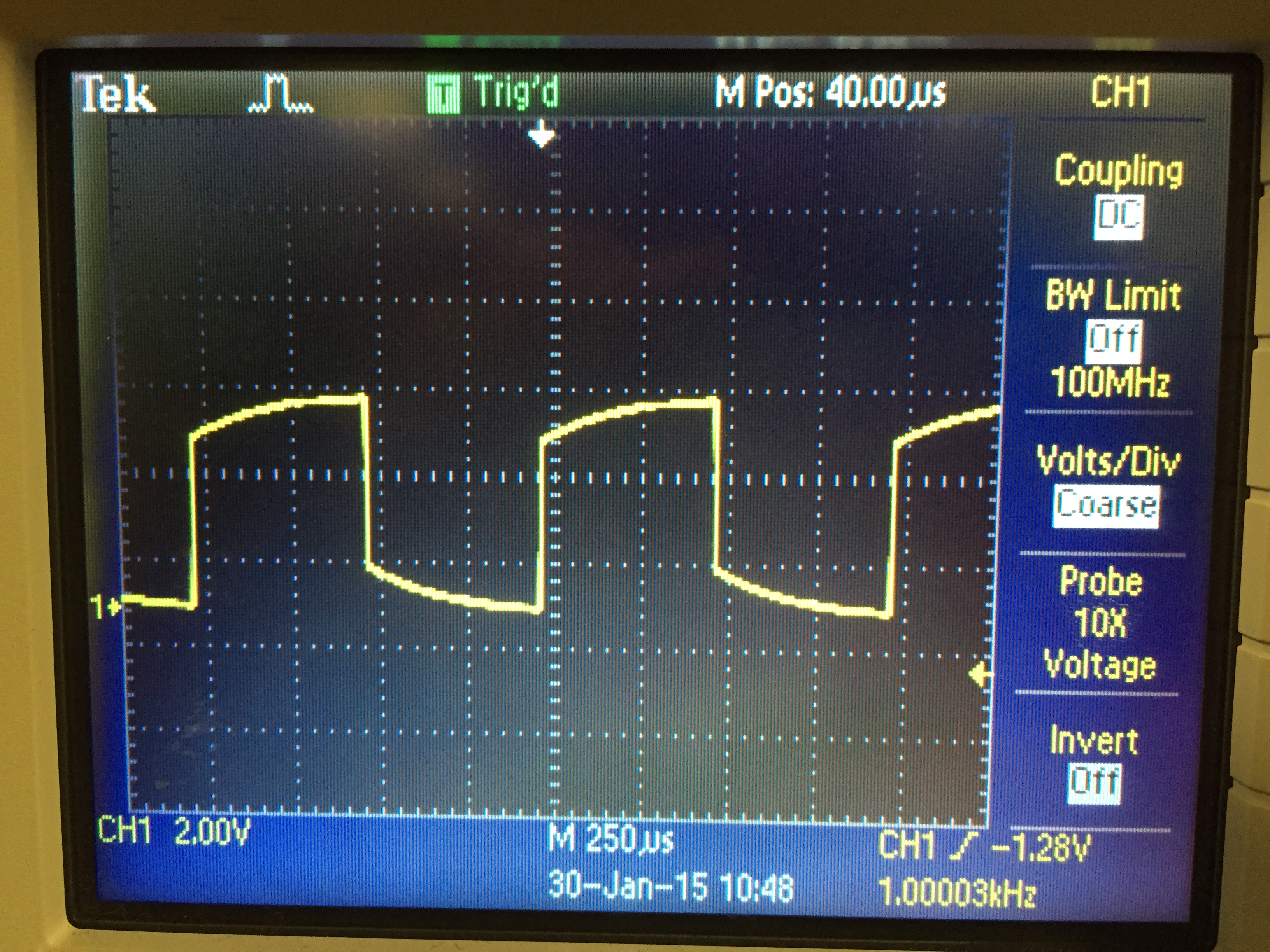
Figure 1b.
| 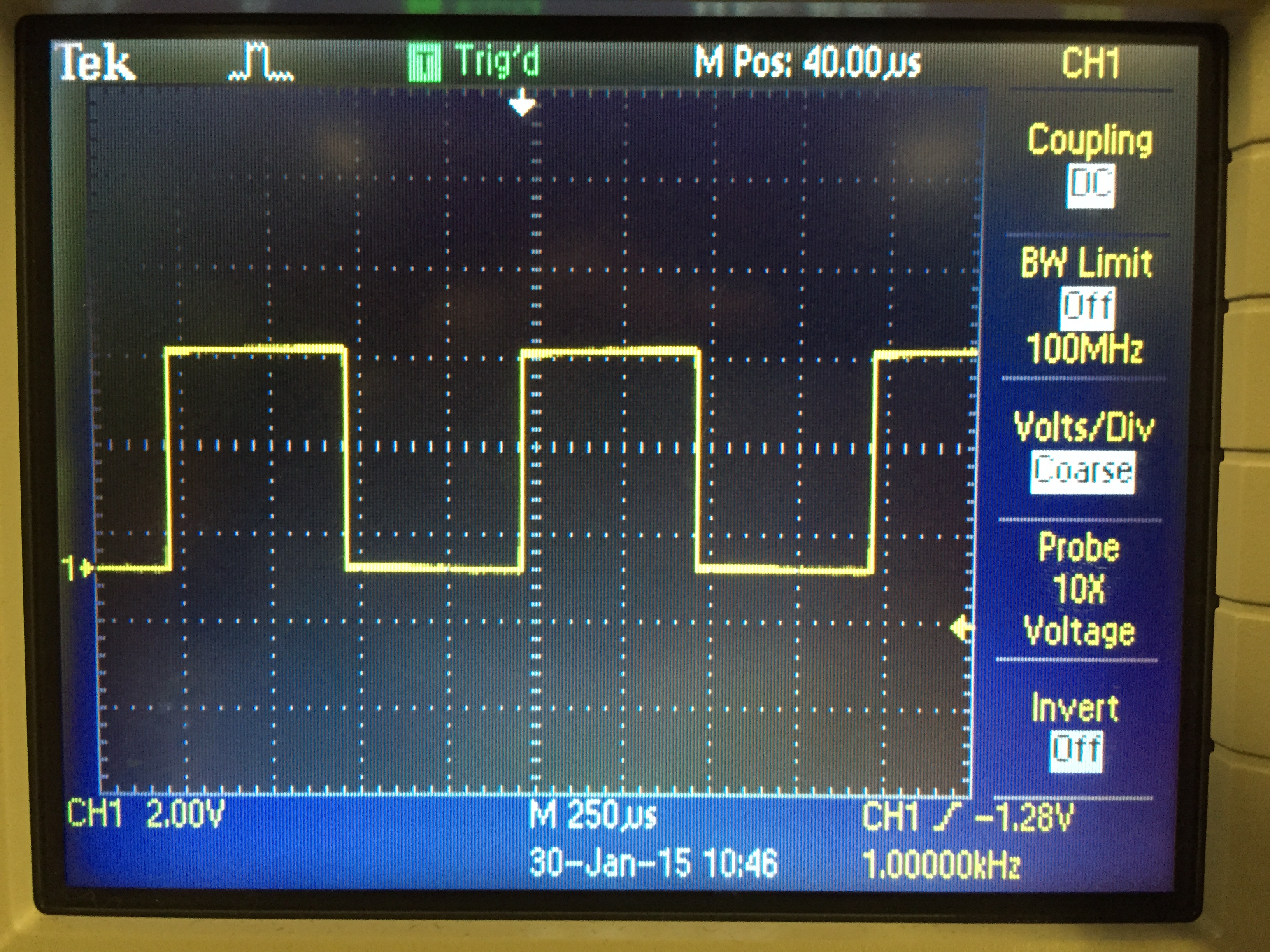
Figure 1c.
|
On the oscilloscope used for this experiment, the probe type is set on the “Channel” menu by selecting the attenuation factor.
The
schematic of a 10:1 scope probe is shown in Figure 1d. Its input
resistance is shown to be 9 M ohm to maintain the 10:1 voltage divider
with the scope, whose input resistance is 1 Mohm. Similarly, the input
capacitance of the probe is chosen to be 12 pF, or one-ninth of the
combined parallel capacitance of the cable and the scope.
The calculation in Figure 1e shows that the input voltage of the scope is indeed one-tenth of the voltage at the probe tip.
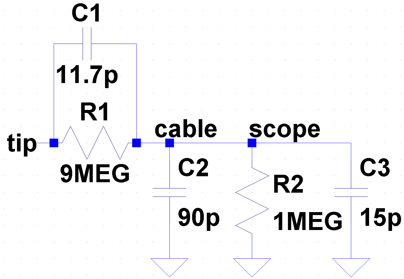
Figure 1d.
| 
Figure 1e.
|
Experiment 2
To
measure the capacitance of a length of cable, the cable can be used as
the capacitor in a series RC circuit and the rise time of its output
measured. The time at which its output reaches 0.5 of the input should
be approximately 0.7 * RC.
For this experiment, an input
square wave of 1 V and a series resistance of 1 M ohm were used. The
halfway rise time was measured to be 104 micros, as shown in Figure 2a.
The calculation in Figure 2b shows that the capacitance of the cable is
149 pF, which approximates the capacitance of 128 pF obtained by a
capacitance meter.

Figure 2a.
| 
Figure 2b. |
Experiment 3
To
demonstrate the difference between compensated and uncompensated
probes, a 0 to 1 V pulse at 1 MHz was applied to a voltage
divider consisting of two 100k resistors. Figures 3a and 3b show the
output of the voltage divider when measured by a compensated scope
probe and an uncompensated cable, respectively.
The
capacitance provided by the compensated probe greatly reduces the total
capacitance seen at the scope input. Thus, the probe output increases
quickly enough to be observed on the scope, even at a high frequency,
as shown in Figure 3a. In contrast, the uncompensated cable causes a
relatively large capacitance to appear at the scope input. Thus,
changes in the cable’s output are negligible on the scope, as shown in
Figure 3b. The cable’s time constant is much greater than that of the
compensated probe.
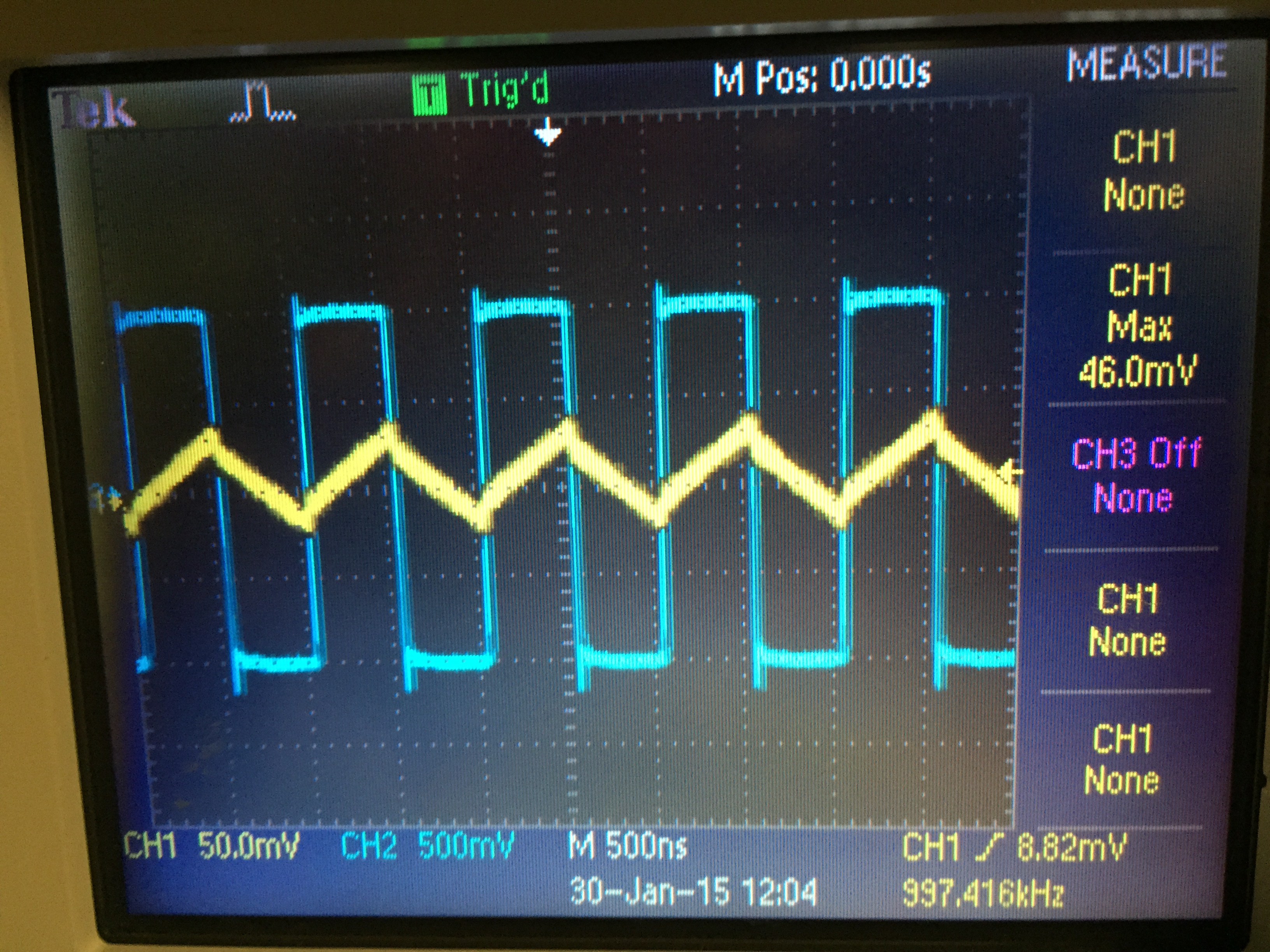
Figure 3a.
| 
Figure 3b.
|
A Final Remark
In
order to directly measure a circuit on a PCB using the uncompensated
cable, a test point must be implemented to prevent the loading effects
seen in Experiment 3. The test point would consist of a large
resistance in parallel with a small capacitance and connected in series
with the cable. The test point imitates the circuitry inside the tip of
a compensated probe, as seen in Figure 1d. The resistance and
capacitance are thus chosen as noted in Experiment 1 to maintain a
desired ratio between the cable’s input and output voltages.
Figures
For Experiment 1:
abc: Laboratory results.
d: Schematic.
e: Calculation.
For Experiment 2:
a: Laboratory result.
b: Calculation.
For Experiment 3:
ab: Laboratory results.
Click to view all labs.