Bad Circuit
Design 6 - Breaking the Feedback Loop around an Op-Amp
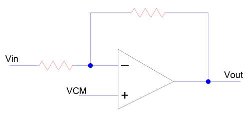
Suppose
we want to implement the simple op-amp circuit seen below using
switched-capacitors (SCs).
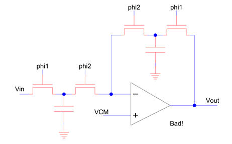
The
schematic seen below is a direct SC implementation, see page 843. The bad
design issue in
this
circuit occurs because there isn’t a continuous path from the output back to
the op-amp’s
input.
When either the phi1- or phi2-controlled switches are off (which is always)
there isn’t
a
feedback path so the op-amp’s outputs will go to the power supply rails.
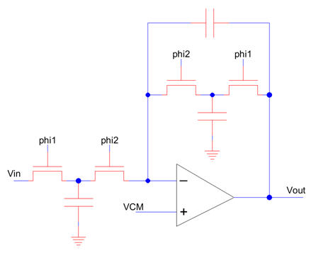
The
fix is to add a capacitor from the output back to the input as seen below. The
added capacitor
provides
a continuous-time feedback path at the cost of speed.
Question,
have we made the bad design mistake discussed in “bad design 5” and not
provided a DC
path
to the input of the op-amp? Answer no. The DC output voltage will be fed back
through the
SC
feedback resistor. It will just take several clock cycles for the circuit to
settle (the DC signal
to
get fed back).
In
simple terms if the only thing connected to the output of the op-amp is a
switch (and a load) then
the
design is likely a “bad design”.