Bad Circuit
Design 10 - Low Power Design: Not Understanding Mismatch
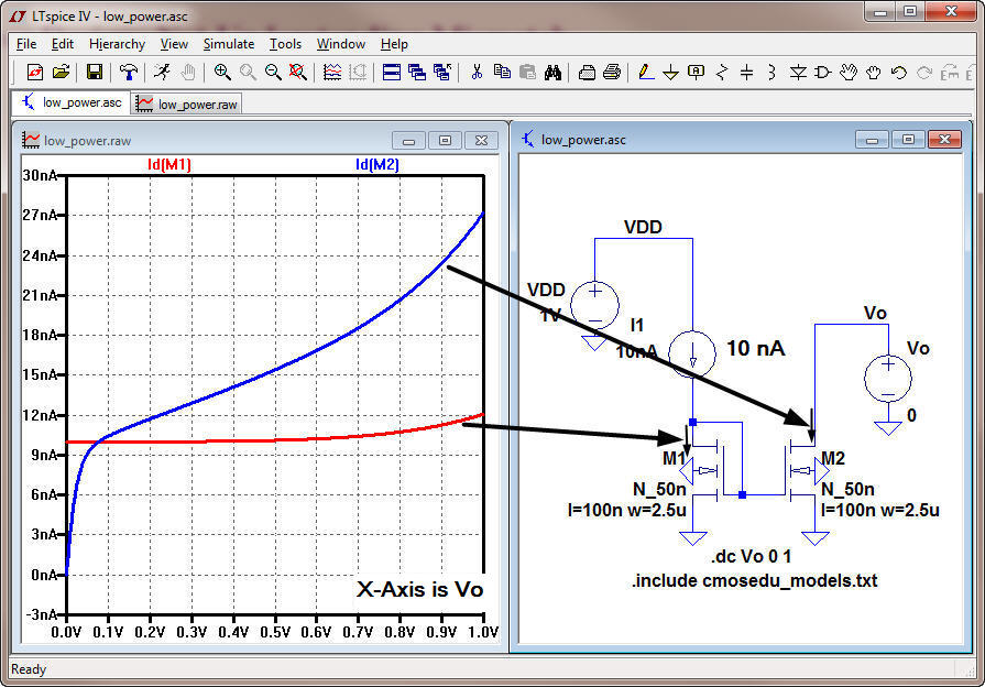
Consider
the current mirror seen below that is biased with a 10 nA
current source. While the reliable
generation
of this 10 nA current using a self-biased reference
is a topic of bad design discussion by itself
we
won’t focus on that here (see page 635). Rather, let’s focus on the current
mirror action. Ideally, M1’s
drain
current is a constant 10 nA; however, because of the gate tunnel current (see page 475) from
M2
the
drain current of M1 increases with larger Vo. This also isn’t the topic of this
bad design discussion.
Neither
is the finite output resistance of M2 resulting in the increase in M2’s drain
current with Vo (up to
27
nA). Rather let’s talk about what happens if M1/M2
aren’t matched (don’t have the same electrical
characteristics
even though they are the same size; they won’t be matched in a real
process….yes, they
will
be matched in SPICE so beware!).
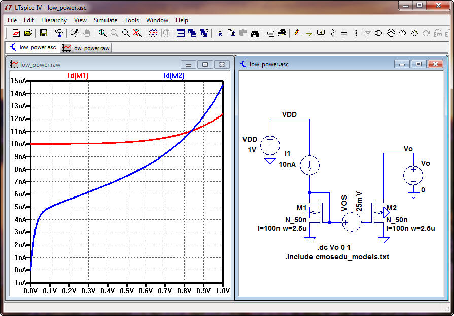
The
gate-source voltage of M1 and M2 is around 75 mV so the devices are operating
in the subthreshold
region.
Remember (page 150) that the drain current in this region is exponentially
dependent on the
gate-source
voltage. So, what happens when we have a modest 25 mV mismatch in the threshold
voltages
between
M1 and M2 (below)? M2 moves towards shutting off. If the other mismatches
(geometry,
mobility,
etc.) are included along with the full range of threshold voltage mismatches
it’s very possible
for
M2 to remain off even though M1 is conducting current.
Perhaps
this isn’t clear enough, in some mirrors M2 will be off (M1 will not be off if a current is forced
through
it). Matching, and slow speed, are fundamental, practical, problems with designing low power
analog
circuits that operate in the subthreshold region.
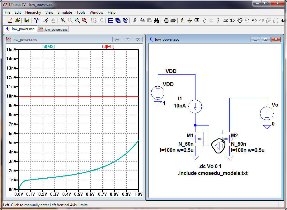
Below
shows the current that flows in M2 with its gate grounded (M2 is “off,” there
isn’t any current
mirror
action). It should be clear that trying to mirror < 1 nA
of current is questionable (see comments
below
about increasing the devices’ gate-source voltage).
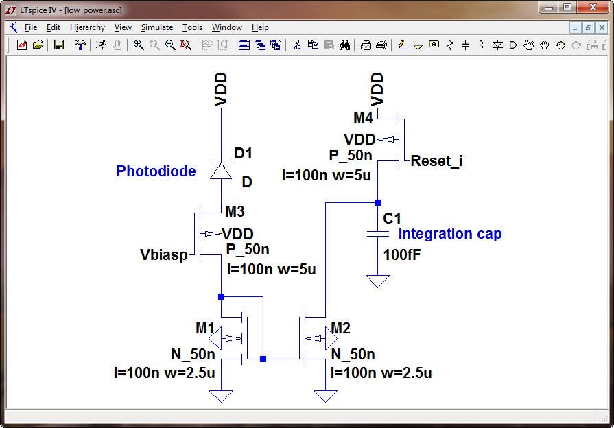
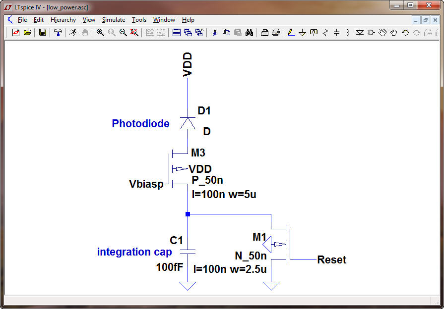
Before
leaving this topic let’s show one more example of bad design, below. The PMOS
device, M3, is
used
to ensure that the voltage across the photodiode stays constant (to keep from
“de-biasing” the
diode).
Mismatches in the characteristics of M3, say a threshold voltage mismatch,
simple change the
voltage
across the diode (which, given that the changes are tens of mV, is rarely a
concern).
The
circuit operates, ideally, as follows. Reset_i goes
low to pre-charge the integration cap. When
Reset_i goes high the diode’s current is mirrored
and discharges the integration capacitor. Larger currents
(more
light) will cause the capacitor to discharge faster (the integration time, the
time between driving
Reset_i high and looking at the voltage across the
integration capacitor, is called the aperture time). We
may
only get pA of current from the photodiode. However, in any case, this circuit
isn’t practical.
This
one, below, will work fine with mismatches (though the Reset is now active high
and the integration
capacitor
is charged instead of discharged by the photo-generated current). It is also a
lower noise design.
Unfortunately,
as discussed on pages 1146-1147, M3 will leak a gate tunneling current onto the
integration
capacitance
resulting in error (so, as discussed on these pages, make sure M3 is as small
as possible).
Note
that by increasing the gate-source voltage of a current mirror operating with
these small currents the
operation
is moved out of the subthreshold region and the chance that M2 shuts off
because of mismatch
is
reduced (see also page 616). This increase in gate-source voltage (overdrive
voltage) is accomplished
by
(significantly) increasing the length of the devices (of course decreasing the
width also helps).
Unfortunately,
besides the hit on layout area, this increase in area will also result in an
increase in the
gate
tunnel current in nanometer CMOS (so, if possible, use older CMOS technology to
design low power
analog
circuits in the subthreshold region).
In simple terms if a design has current
mirrors that mirror pA or a few nA of current be
skeptical, be very
skeptical, because the design is likely a
bad design.